

Schematic editor
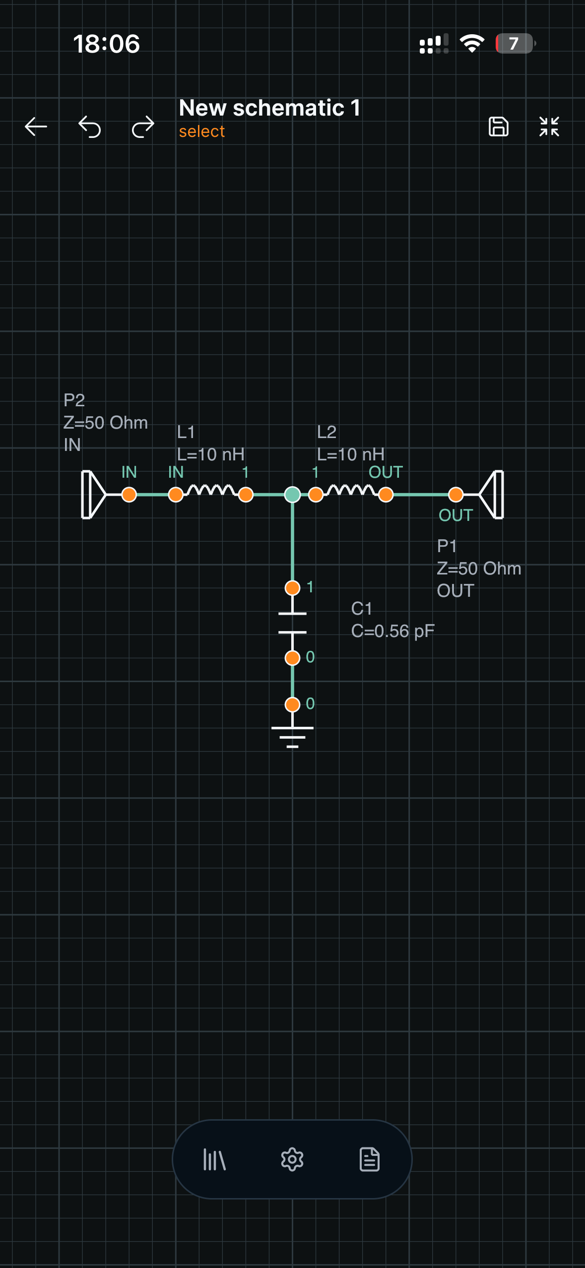
Schematic editor
Draw analog and RF circuits with ports, components, net labels, and touch-friendly editing.
Design, simulate, measure, and optimize electronic circuits across desktop, tablet, and mobile.
Product proof
Build a schematic, choose an analysis, add measurements, and tune values without leaving your device.
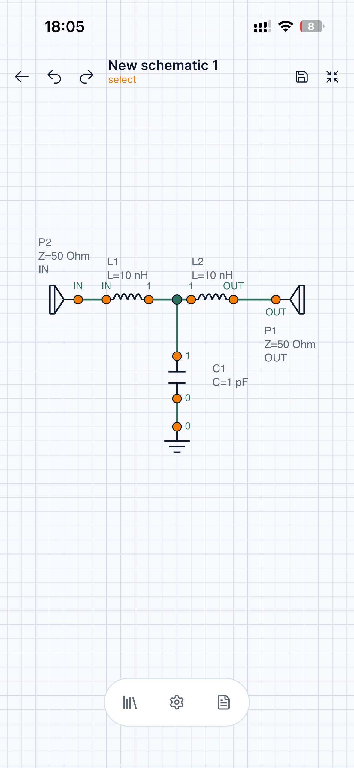
Draw analog and RF circuits with ports, components, net labels, and touch-friendly editing.
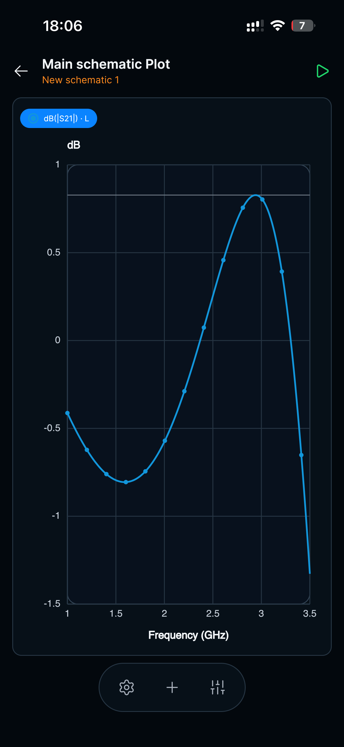
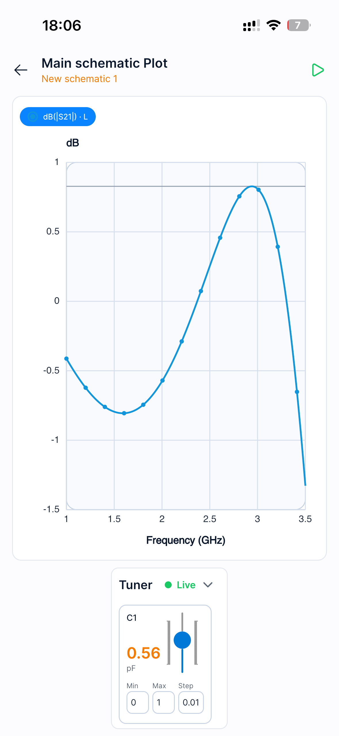
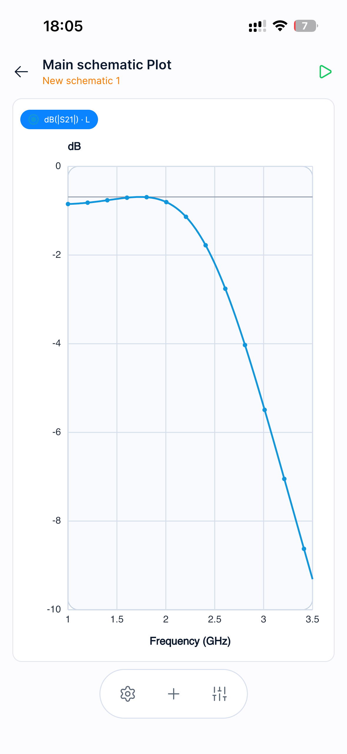
Inspect traces, markers, frequency response, and derived measurements.
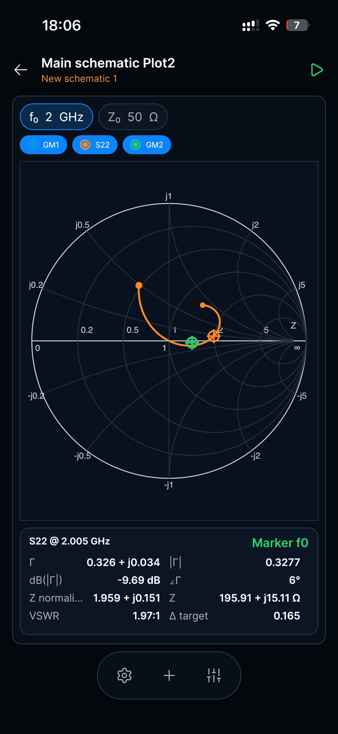
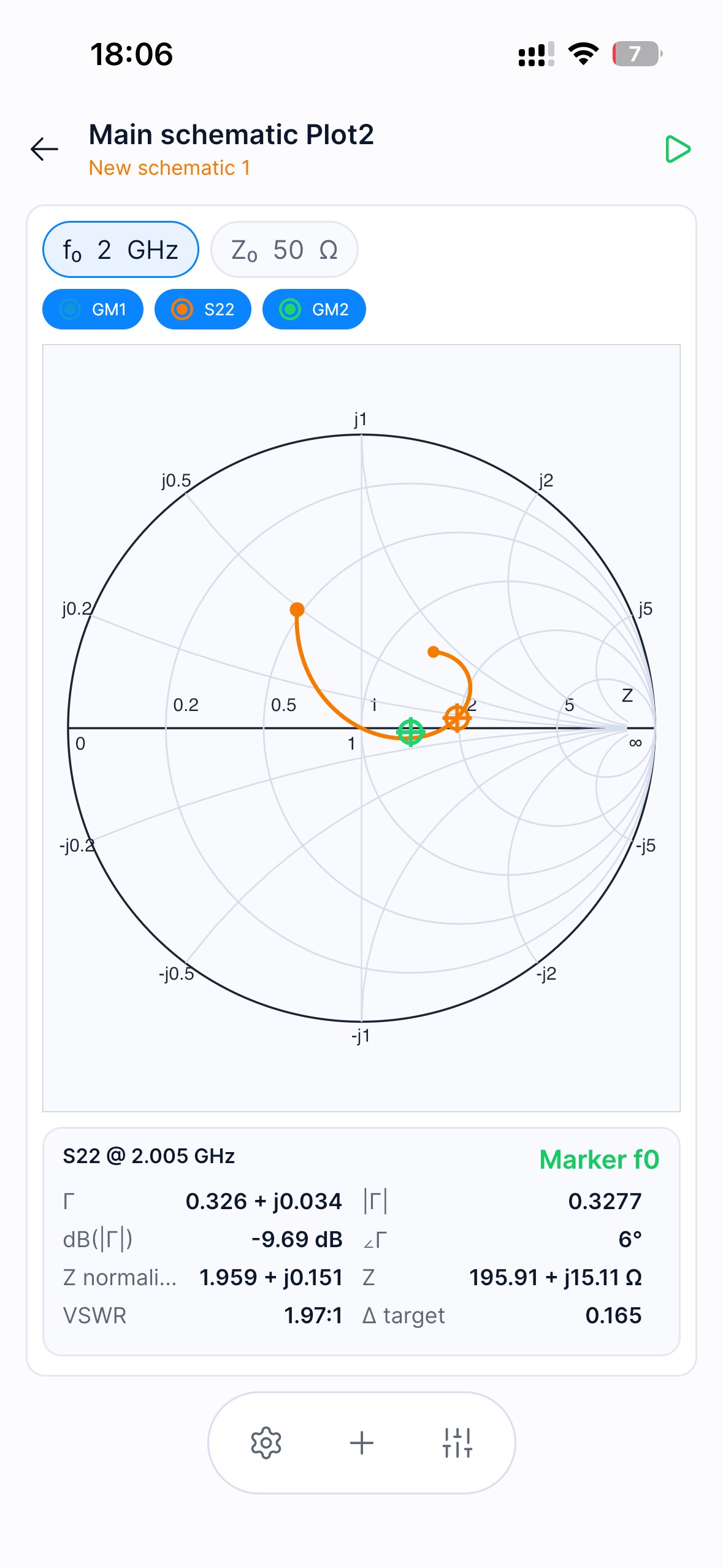
Analyze S-parameters, return loss, insertion loss, impedance, and Smith chart trajectories.
Updated July 27, 2026
Tersa EDA is an RF and analog circuit simulation workspace for engineers, students, and hardware teams who need a focused schematic-to-measurement flow. It combines schematic capture, SPICE-compatible analysis setup, plots, RF measurements, Smith chart inspection, and component tuning in one product surface. The goal is not to replace large desktop EDA suites. The product is designed for quick experiments, tablet review, mobile debugging, and focused circuit tuning when the important question is how the response changes after a component value, port, or measurement is adjusted.
Tersa EDA presents RF results around practical measurements: S11, S21, S12, S22, return loss, insertion loss, gain, stability-oriented traces, frequency markers, and Smith chart trajectories. The workflow starts from the schematic, adds ports and analysis settings, then keeps the plot and tuner connected to the circuit. This makes it useful for filters, matching networks, resonators, small-signal experiments, and quick RF review where the designer needs to compare traces instead of exporting data between separate tools.
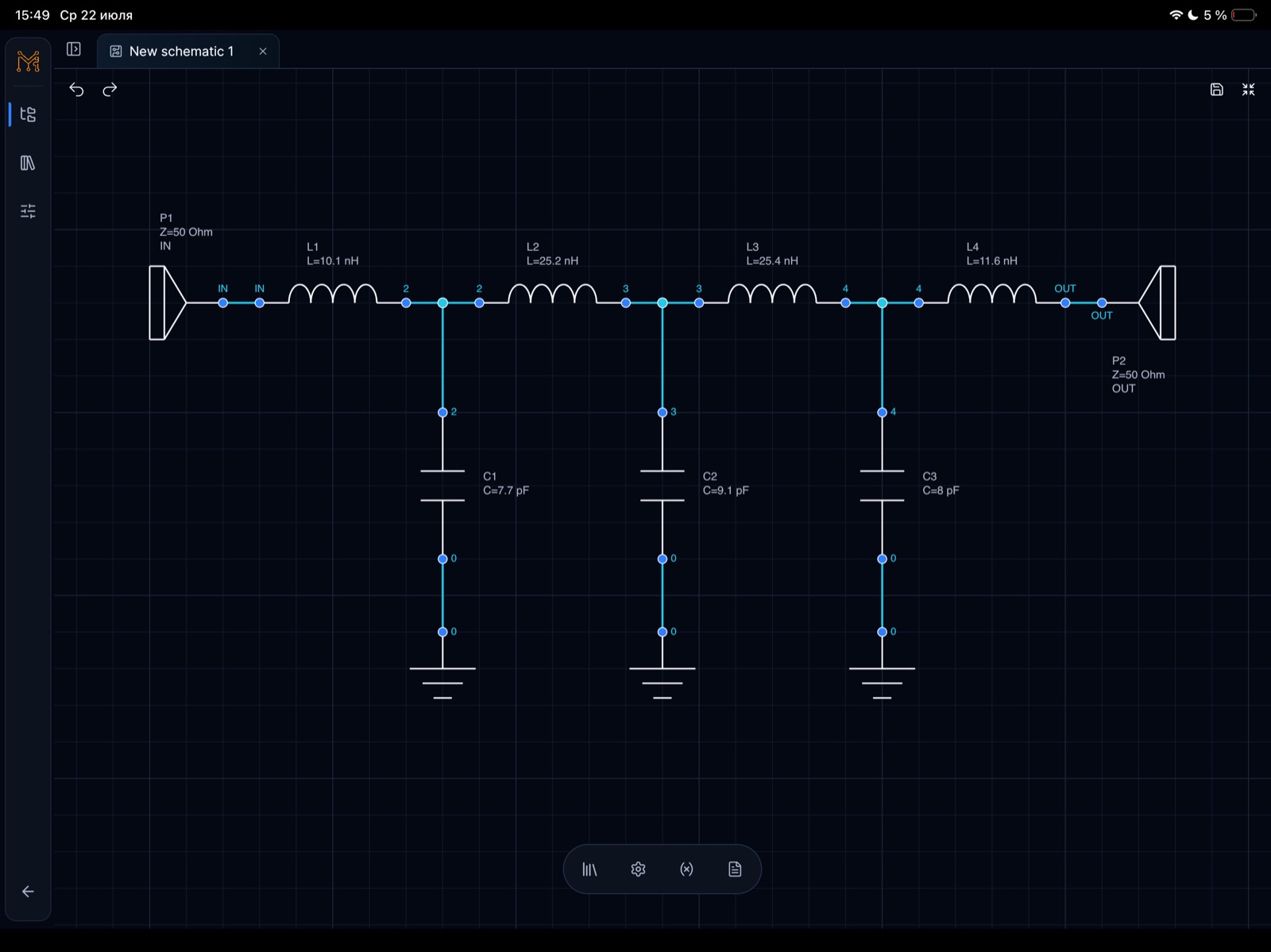
The 500 MHz low-pass filter example demonstrates a complete RF workflow on iPad. It shows a 50 ohm ladder filter with series inductors, shunt capacitors, input and output ports, S-parameter simulation to 1 GHz, insertion loss, return loss, and component tuning. The blue S21 trace shows passband behavior and roll-off, while the green S11 and S22 traces help inspect matching. The tuning sweep makes cutoff movement visible as capacitor and inductor values change around the target frequency.
Features
Create circuits with components, ports, labels, and reusable sheets on mobile, tablet, or desktop.
Run AC, transient, and RF analyses with clean plots, markers, and trace controls.
Inspect S-parameters, return loss, insertion loss, Smith charts, gain, and stability metrics.
Tune component values and immediately see how the circuit response changes.
Workflow
Build a schematic, choose an analysis, add measurements, and tune values without leaving your device.
Place components, connect nets, and define ports.
Run AC, transient, or RF simulations.
Plot voltages, S-parameters, losses, and markers.
Adjust components and compare the response.
Product demos
Short product videos show schematic creation, simulation, measurement, and live component tuning in Tersa EDA.
Tune an RLC circuit directly on iPhone and watch the response update while component values change.
Open on YouTubeCreate an RLC schematic on iPhone, run simulation, and inspect the first measurement workflow.
Open on YouTubeUse the iPad workspace to tune resonance and compare circuit response changes on a larger engineering canvas.
Open on YouTubeBuild an RLC resonator from scratch on iPad and move from schematic capture into analysis setup.
Open on YouTubeRF example
A concrete LPF case study built in Tersa EDA: schematic capture, 50 ohm ports, S-parameter simulation, insertion loss, return loss, and component tuning around a 500 MHz target.
Target
500 MHz LPF
Ports
50 ohm IN / OUT
Analysis
S-parameters to 1 GHz
Workflow
Schematic, plot, tuner
This example shows a lumped 500 MHz low-pass filter workflow, not a generic screenshot gallery. The circuit uses a ladder topology with 50 ohm input and output ports, series inductors, shunt capacitors, and RF measurements plotted from DC to 1 GHz.
The blue S21 trace shows the passband and roll-off, while the green S11/S22 traces help inspect matching and return loss. Tuning sweeps make cutoff movement visible as component values change.
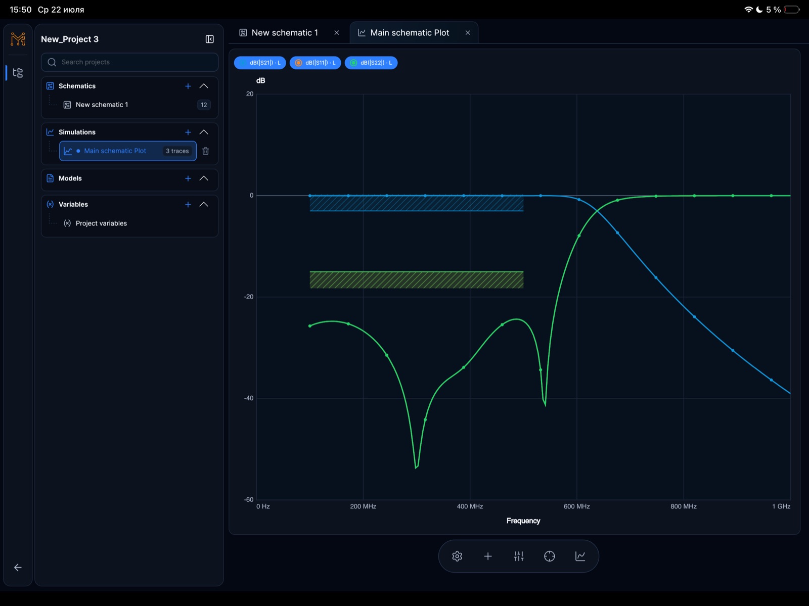
S-parameter response with S21 staying flat through the passband before the transition region toward 1 GHz.
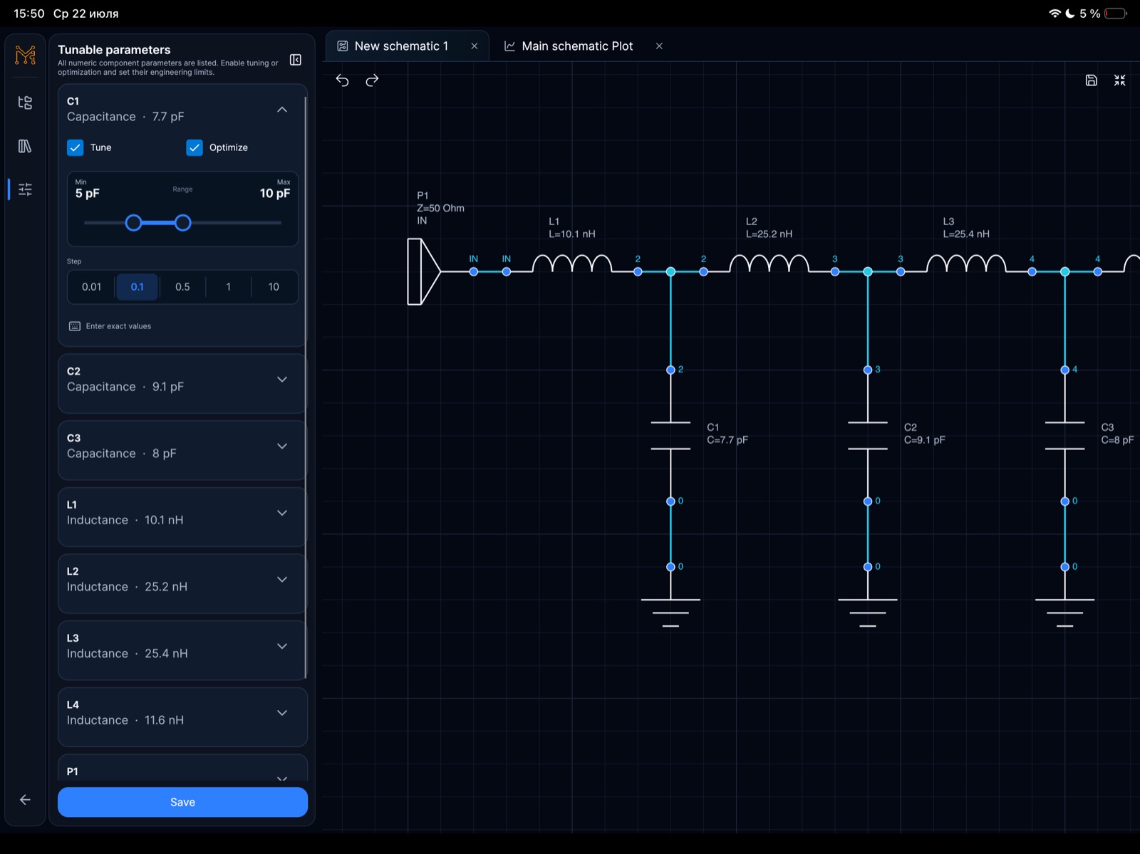
Tuning ranges expose capacitor and inductor values so the cutoff behavior can be optimized directly from the schematic.
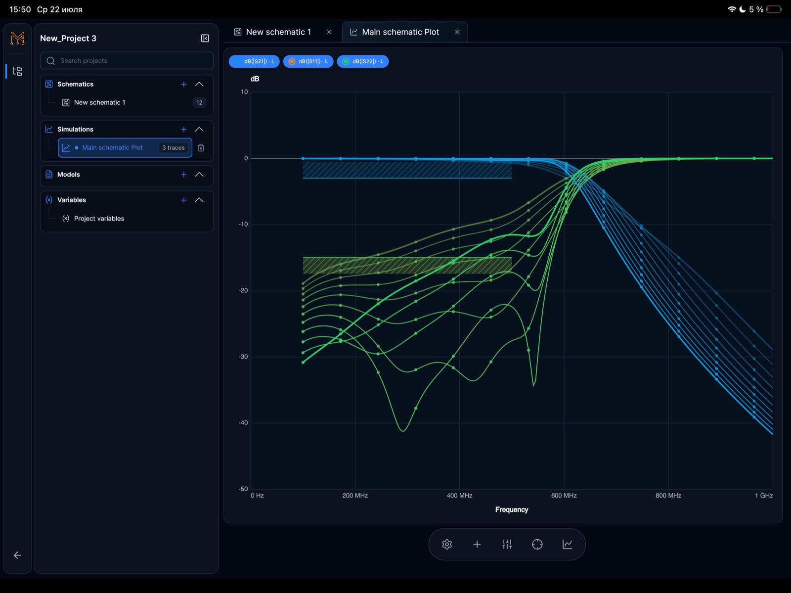
A tuning sweep compares multiple S-parameter traces around the cutoff and stopband regions.
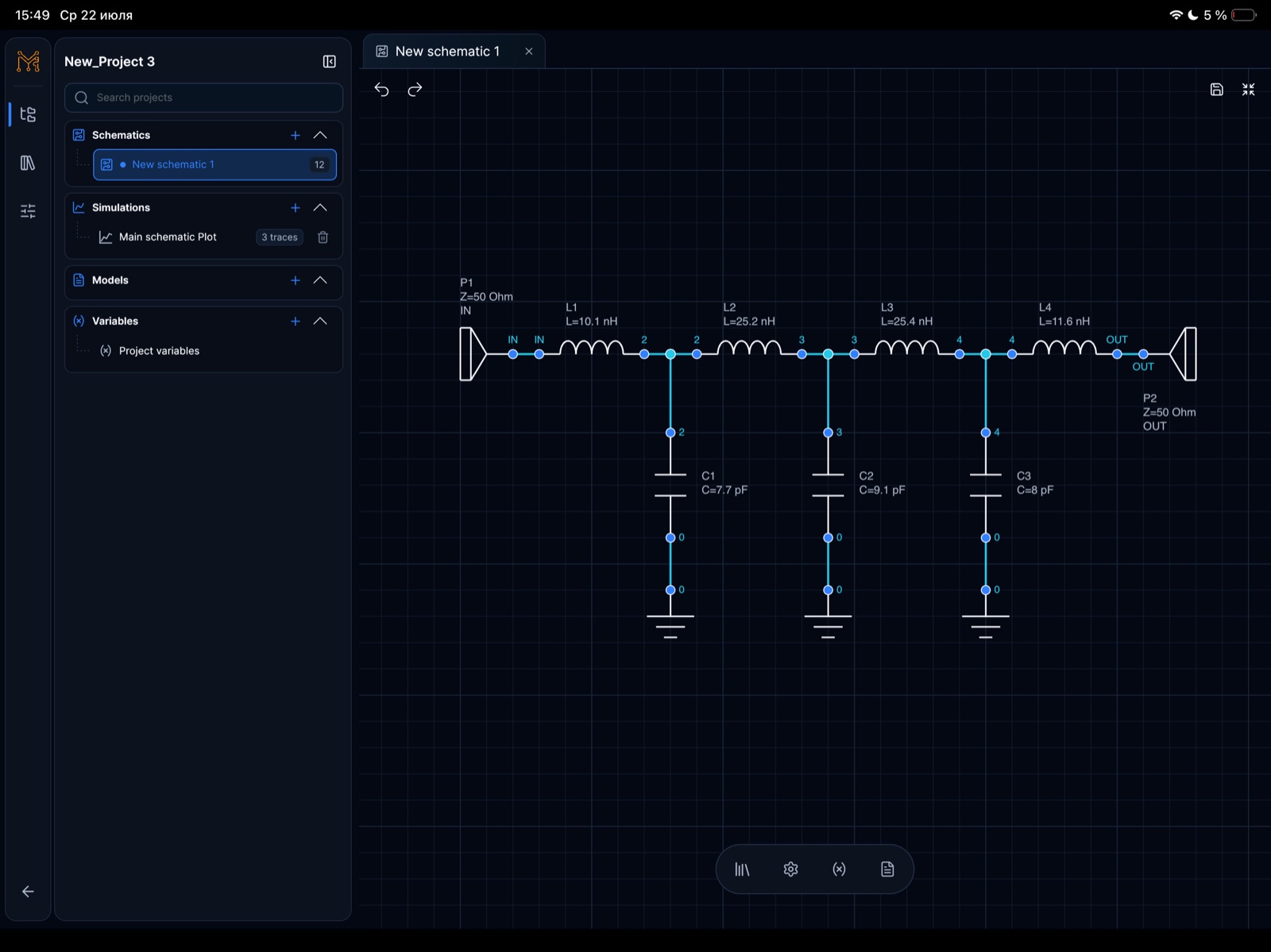
The project workspace keeps the LPF schematic, simulation plot, variables, and tunable parameters in one engineering flow.
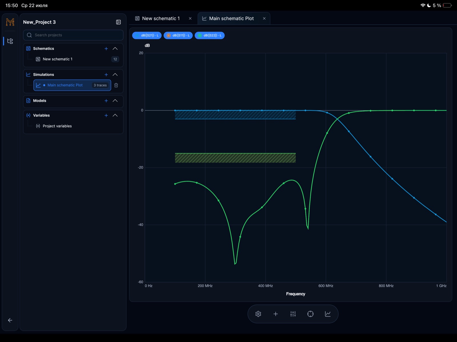
Return loss and insertion loss traces make it possible to inspect passband fit and out-of-band rejection.
RF Tools
Tersa EDA includes RF-focused measurements alongside everyday analog simulation: S-parameters, return loss, insertion loss, Smith chart trajectories, gain metrics, stability factors, and target-frequency markers.
Analog
Use Tersa EDA for filters, dividers, amplifiers, diode circuits, RC transients, frequency response checks, and quick what-if experiments.
Screenshots
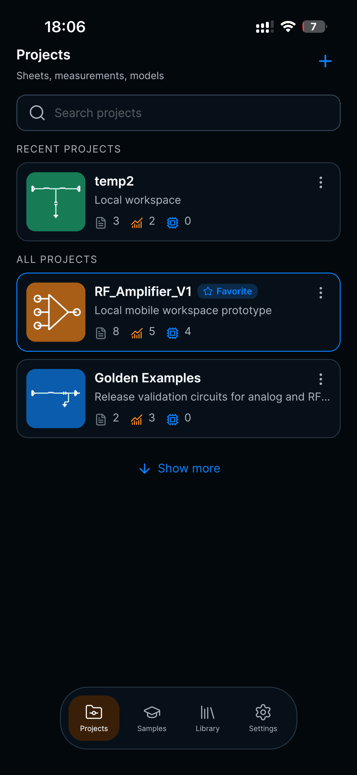
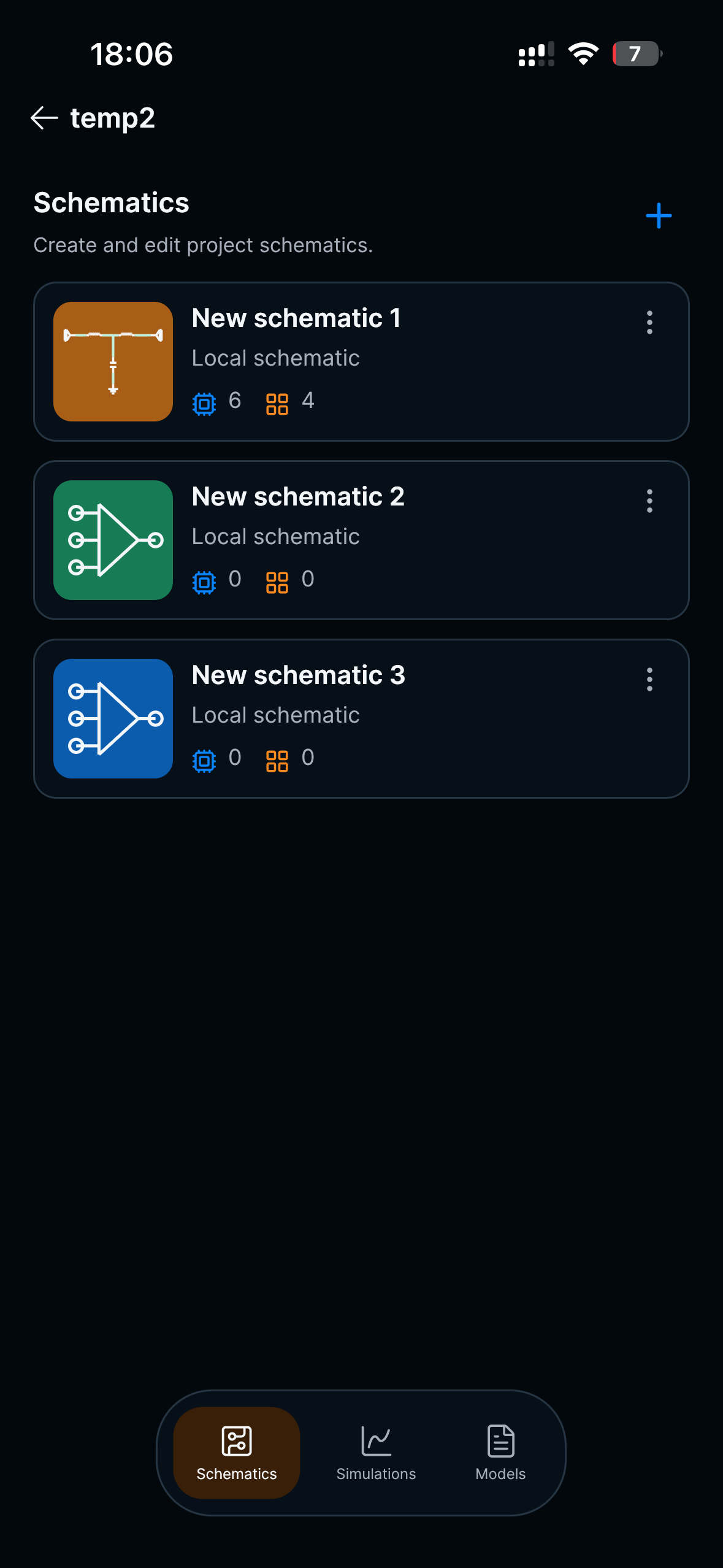
Real app screens from projects, schematic editing, RF plots, Smith chart inspection, and tuning.
Beta testing
We are inviting engineers, students, and RF/analog teams to try early builds and tell us what should be sharpened first.
Not yet. Tersa EDA focuses on schematic capture, circuit simulation, measurements, plots, and analog/RF tuning.
No. It is a lightweight workspace for quick circuit experiments, mobile review, and RF/analog tuning. It is designed to complement desktop engineering tools.
The first versions focus on analog circuits, AC and transient analysis, S-parameters, Smith charts, and component tuning.
No. The interface is designed for mobile, tablet, and desktop screens.
Tersa EDA uses a SPICE-compatible simulation workflow for circuit analysis.