

회로도 편집기
회로도 편집기
포트, 부품, net label, 터치 친화적 편집으로 아날로그 및 RF 회로를 그립니다.
Tersa EDA · RF / analog
Tersa EDA은 회로도를 만들고, 회로 시뮬레이션을 실행하며, 부품을 조정하고 RF 측정을 확인하는 모바일 및 데스크톱 앱입니다.
제품 증거
회로도를 만들고, 분석을 선택하고, 측정을 추가하고, 장치를 떠나지 않고 값을 조정하세요.
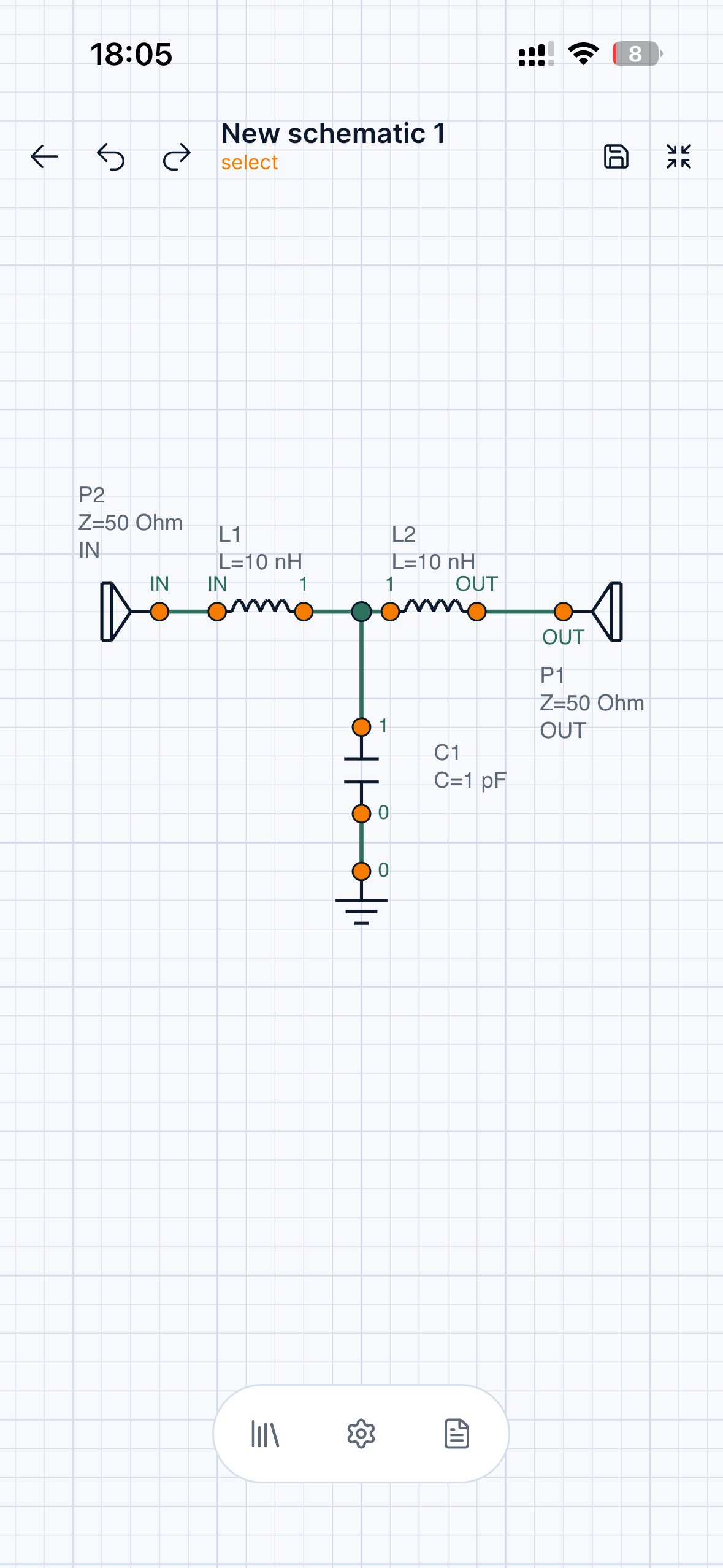
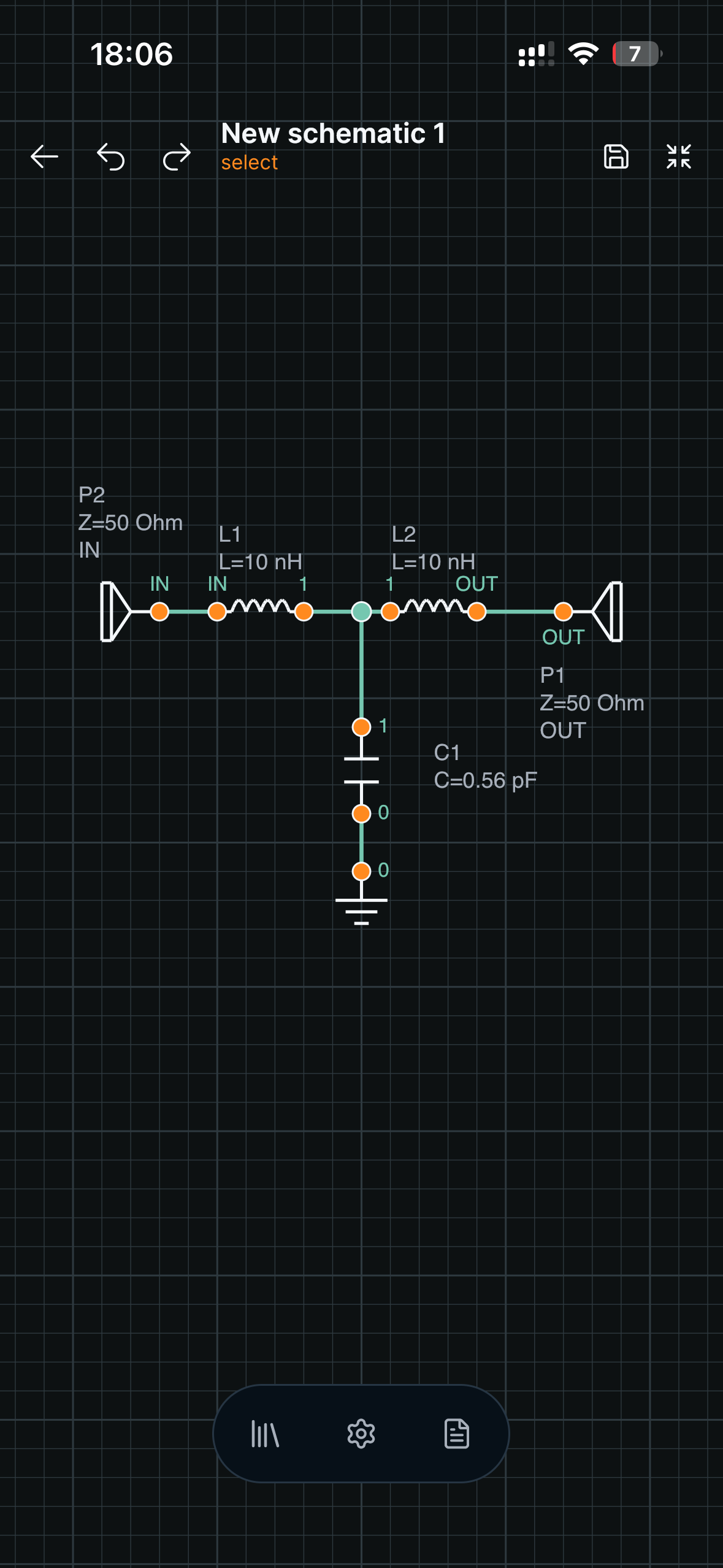
회로도 편집기
포트, 부품, net label, 터치 친화적 편집으로 아날로그 및 RF 회로를 그립니다.
측정
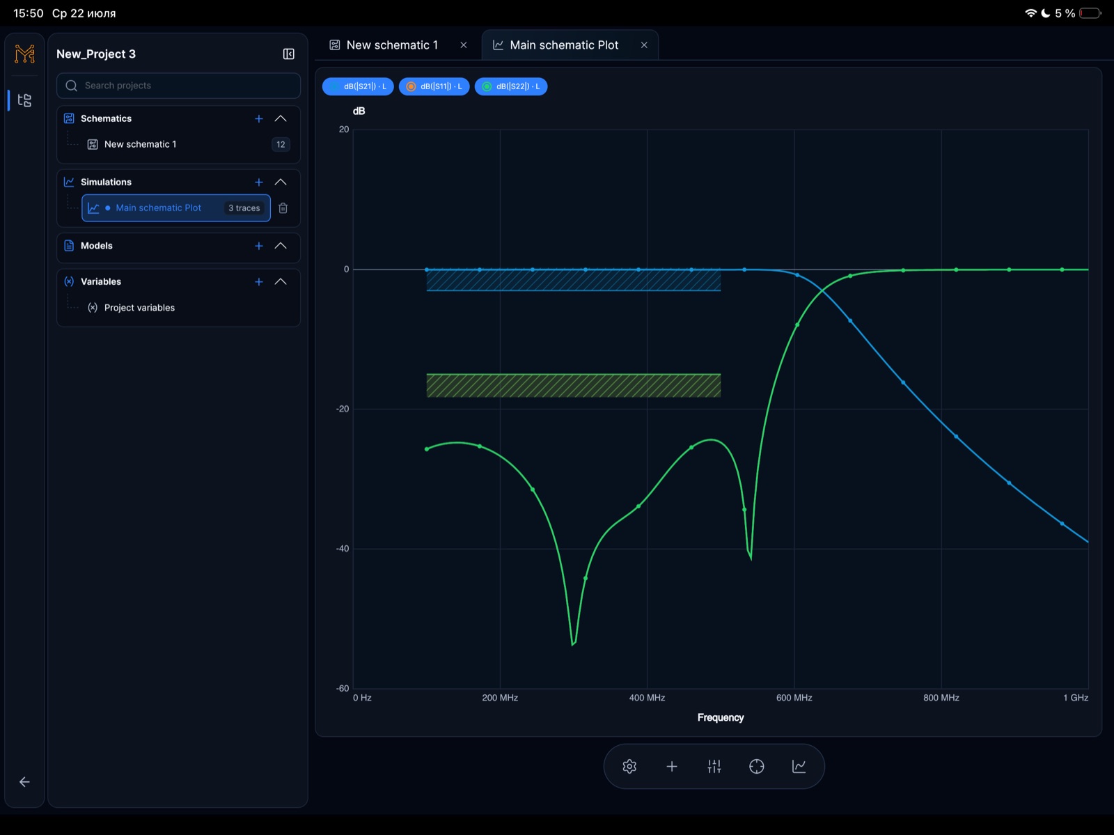
트레이스, 마커, 주파수 응답, 파생 측정을 확인합니다.
RF
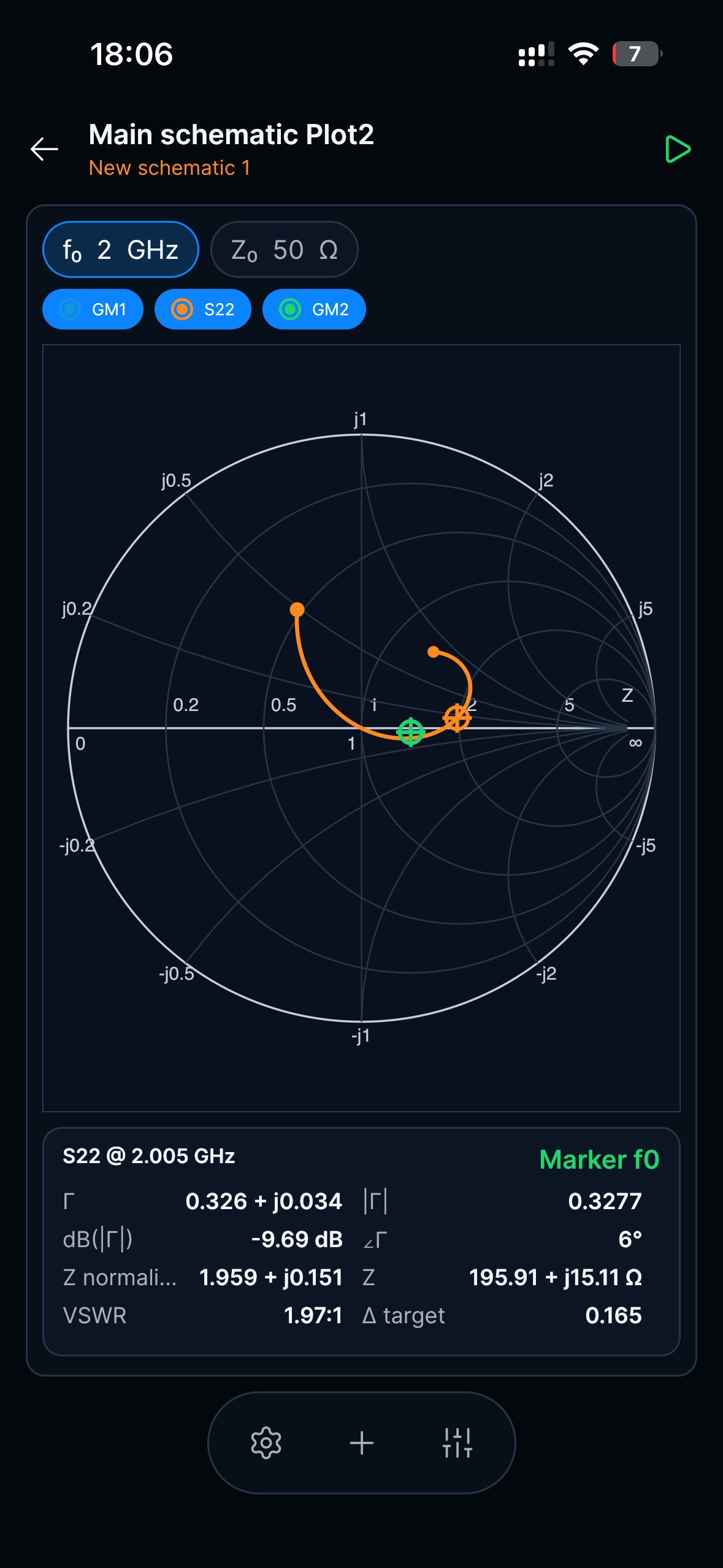
S-파라미터, return loss, insertion loss, 임피던스, Smith 차트 궤적을 분석합니다.
Updated July 27, 2026
Tersa EDA is an RF and analog circuit simulation workspace for engineers, students, and hardware teams who need a focused schematic-to-measurement flow. It combines schematic capture, SPICE-compatible analysis setup, plots, RF measurements, Smith chart inspection, and component tuning in one product surface. The goal is not to replace large desktop EDA suites. The product is designed for quick experiments, tablet review, mobile debugging, and focused circuit tuning when the important question is how the response changes after a component value, port, or measurement is adjusted.
Tersa EDA presents RF results around practical measurements: S11, S21, S12, S22, return loss, insertion loss, gain, stability-oriented traces, frequency markers, and Smith chart trajectories. The workflow starts from the schematic, adds ports and analysis settings, then keeps the plot and tuner connected to the circuit. This makes it useful for filters, matching networks, resonators, small-signal experiments, and quick RF review where the designer needs to compare traces instead of exporting data between separate tools.
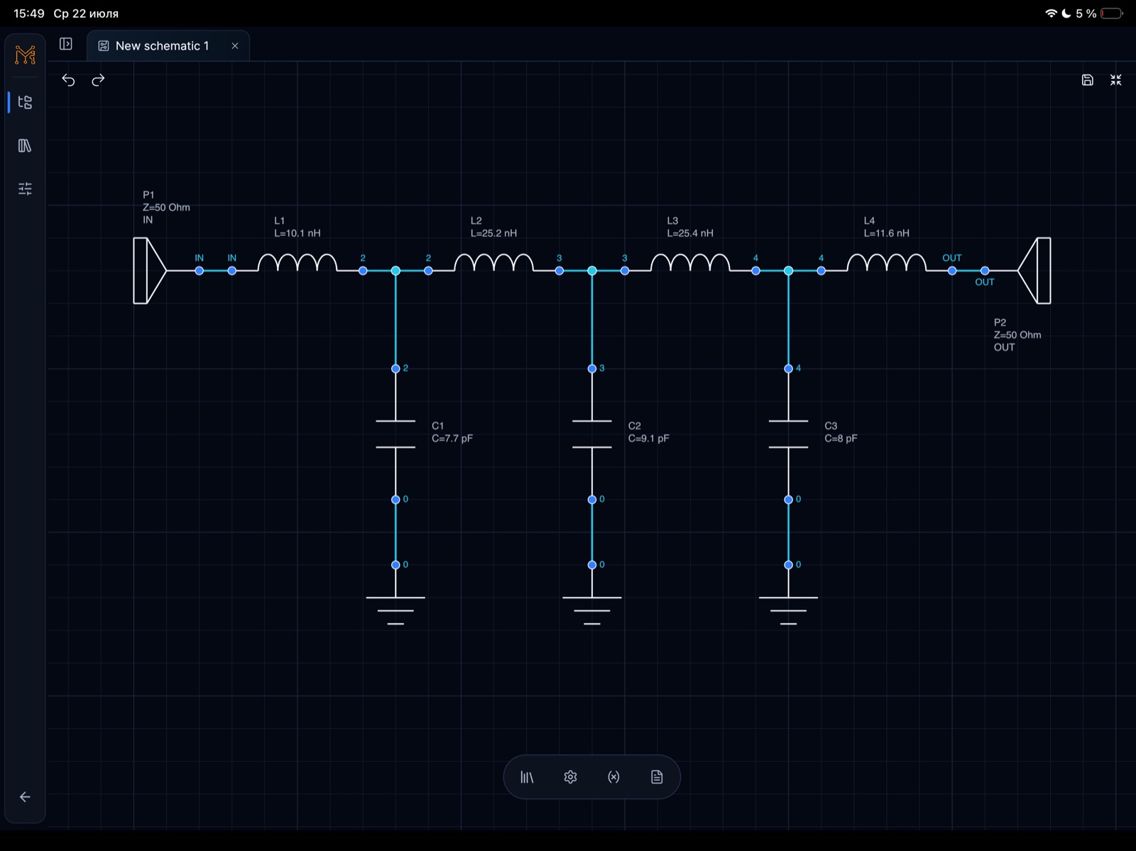
The 500 MHz low-pass filter example demonstrates a complete RF workflow on iPad. It shows a 50 ohm ladder filter with series inductors, shunt capacitors, input and output ports, S-parameter simulation to 1 GHz, insertion loss, return loss, and component tuning. The blue S21 trace shows passband behavior and roll-off, while the green S11 and S22 traces help inspect matching. The tuning sweep makes cutoff movement visible as capacitor and inductor values change around the target frequency.
기능
모바일, 태블릿, 데스크톱에서 부품, 포트, 라벨, 재사용 가능한 시트로 회로를 만듭니다.
명확한 플롯, 마커, 트레이스 제어로 AC, 과도, RF 분석을 실행합니다.
S-파라미터, return loss, insertion loss, Smith 차트, gain, 안정도 지표를 확인합니다.
부품 값을 조정하고 회로 응답이 어떻게 변하는지 즉시 확인합니다.
SPICE simulation, typed measurement, 제한형 optimization, Touchstone 1.x, 편집 가능한 회로 생성은 production에서 운영 중입니다. harmonic balance, EM, 더 넓은 RF synthesis는 roadmap입니다.
https://mcp-api.tersaeda.com/mcp · OAuth 2.1 + PKCE
현재 사용 가능
Live beta격리된 ngspice worker에서 검증된 .op/.dc/.ac/.tran/.noise 분석과 제한된 vectors, 안정적 진단을 제공합니다.
플랫폼 roadmap
Harmonic balance
연구
EM 분석
계획
Roadmap 항목은 제품 방향이며 현재 사용할 수 있는 MCP tools가 아닙니다. 범위와 출시 순서는 변경될 수 있습니다.
워크플로
회로도를 만들고, 분석을 선택하고, 측정을 추가하고, 장치를 떠나지 않고 값을 조정하세요.
부품을 배치하고 net을 연결하고 포트를 정의합니다.
AC, 과도 또는 RF 시뮬레이션을 실행합니다.
전압, S-파라미터, 손실, 마커를 플롯합니다.
부품을 조정하고 응답을 비교합니다.
Product demos
짧은 영상에서 Tersa EDA의 회로도 생성, 시뮬레이션, 측정, 실시간 부품 튜닝을 볼 수 있습니다.
Tune an RLC circuit directly on iPhone and watch the response update while component values change.
YouTube에서 열기Create an RLC schematic on iPhone, run simulation, and inspect the first measurement workflow.
YouTube에서 열기Use the iPad workspace to tune resonance and compare circuit response changes on a larger engineering canvas.
YouTube에서 열기Build an RLC resonator from scratch on iPad and move from schematic capture into analysis setup.
YouTube에서 열기RF example
A concrete LPF case study built in Tersa EDA: schematic capture, 50 ohm ports, S-parameter simulation, insertion loss, return loss, and component tuning around a 500 MHz target.
Target
500 MHz LPF
Ports
50 ohm IN / OUT
Analysis
S-parameters to 1 GHz
Workflow
Schematic, plot, tuner
This example shows a lumped 500 MHz low-pass filter workflow, not a generic screenshot gallery. The circuit uses a ladder topology with 50 ohm input and output ports, series inductors, shunt capacitors, and RF measurements plotted from DC to 1 GHz.
The blue S21 trace shows the passband and roll-off, while the green S11/S22 traces help inspect matching and return loss. Tuning sweeps make cutoff movement visible as component values change.
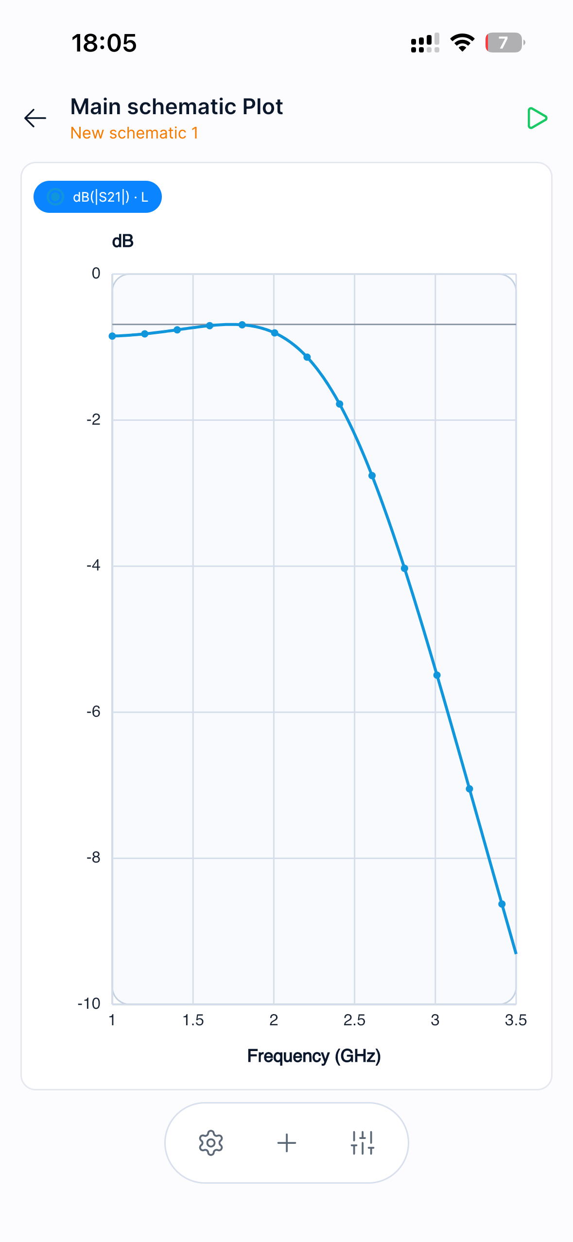
S-parameter response with S21 staying flat through the passband before the transition region toward 1 GHz.
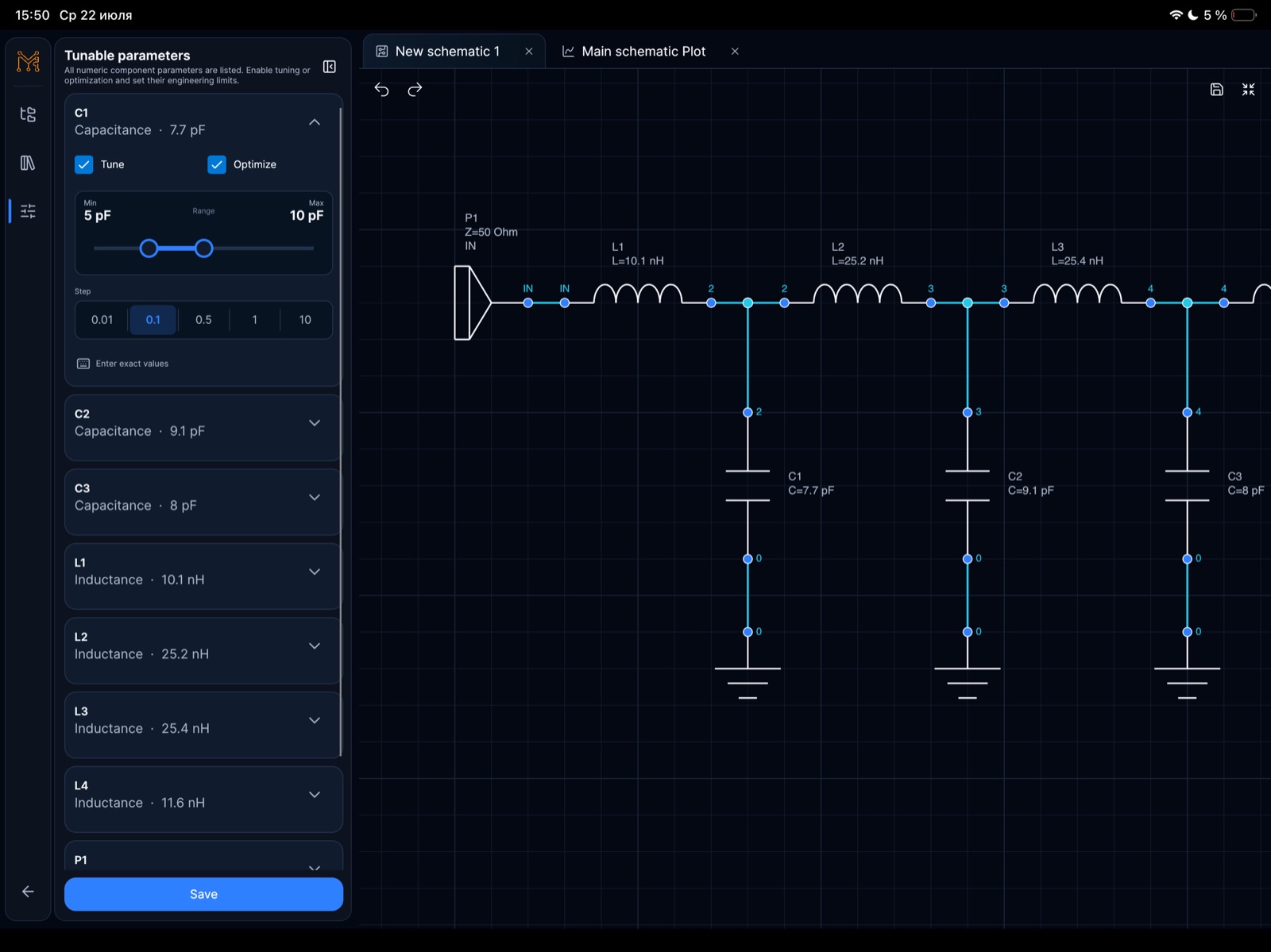
Tuning ranges expose capacitor and inductor values so the cutoff behavior can be optimized directly from the schematic.
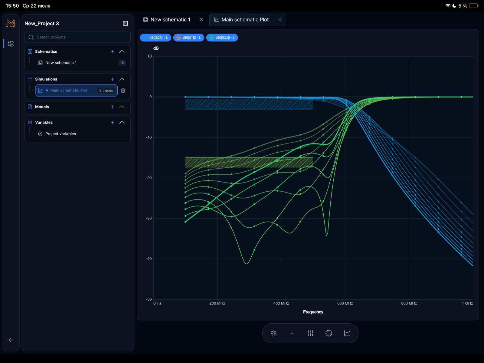
A tuning sweep compares multiple S-parameter traces around the cutoff and stopband regions.
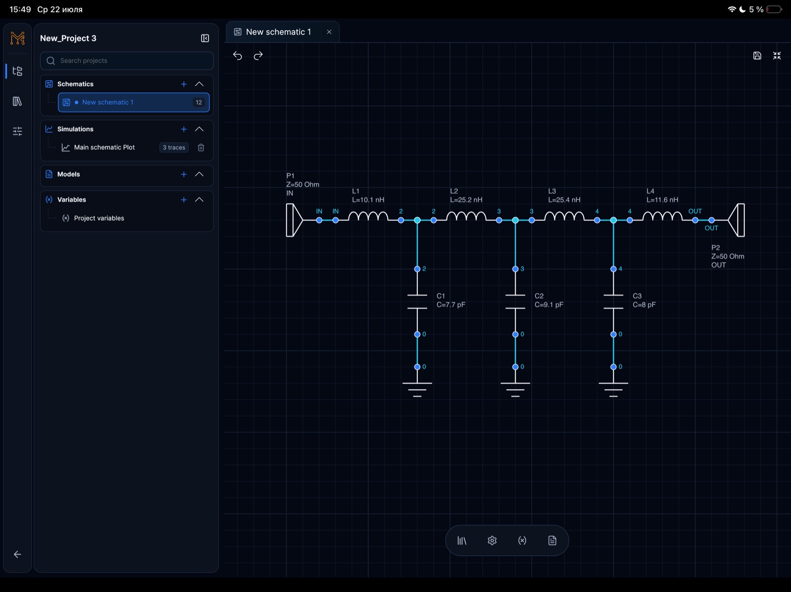
The project workspace keeps the LPF schematic, simulation plot, variables, and tunable parameters in one engineering flow.
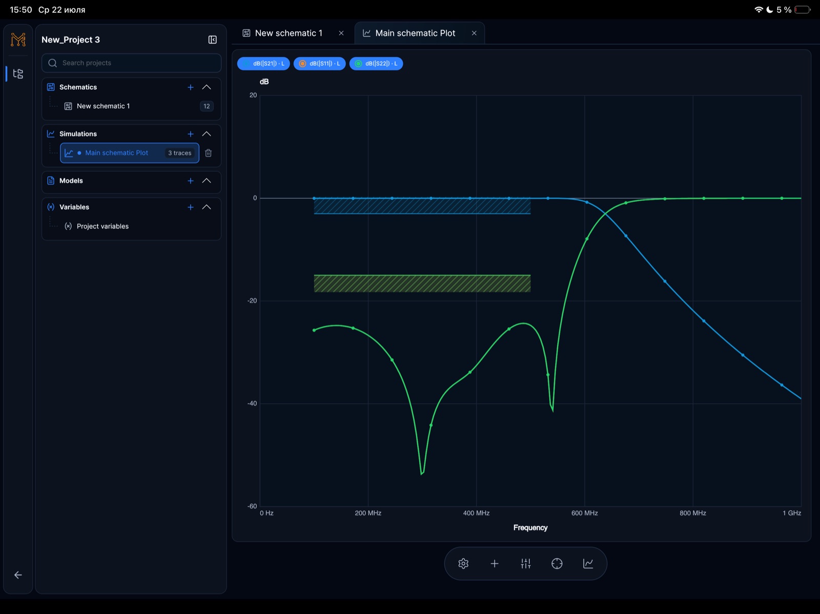
Return loss and insertion loss traces make it possible to inspect passband fit and out-of-band rejection.
RF 도구
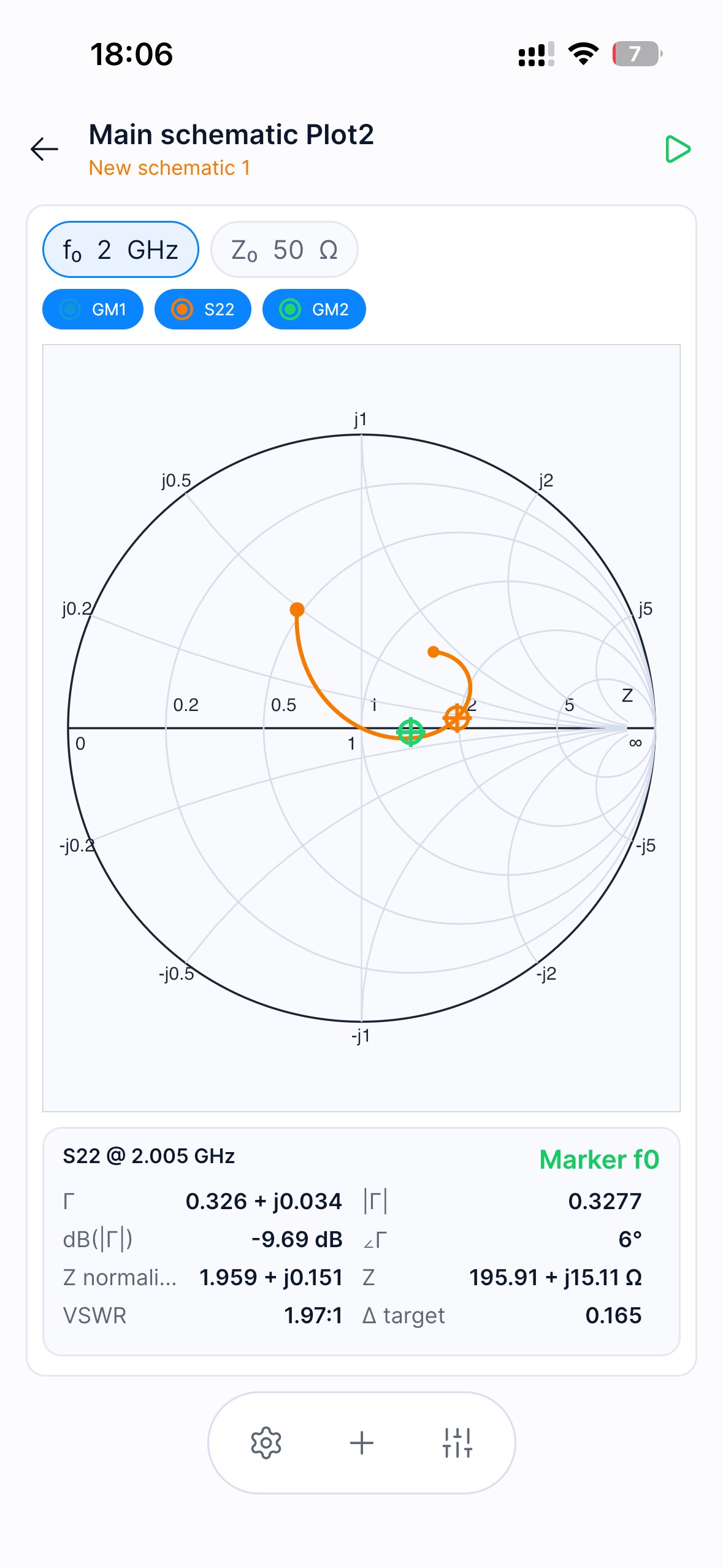
Tersa EDA은 일상적인 아날로그 시뮬레이션 옆에 S-파라미터, return loss, insertion loss, Smith 차트 궤적, gain, 안정도, 목표 주파수 마커를 제공합니다.
아날로그
필터, 분압기, 증폭기, 다이오드 회로, RC 과도, 주파수 응답 확인, 빠른 what-if 실험에 사용할 수 있습니다.
스크린샷
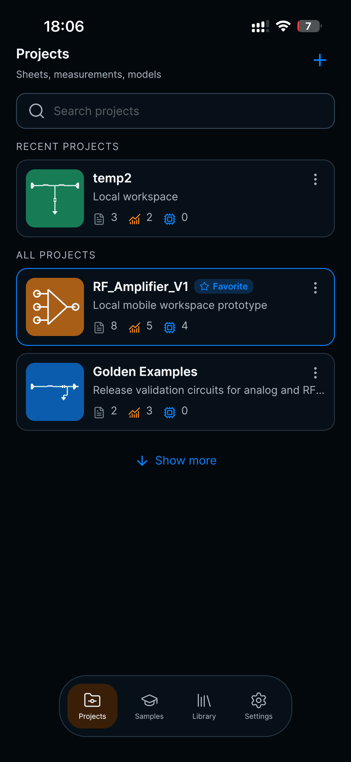
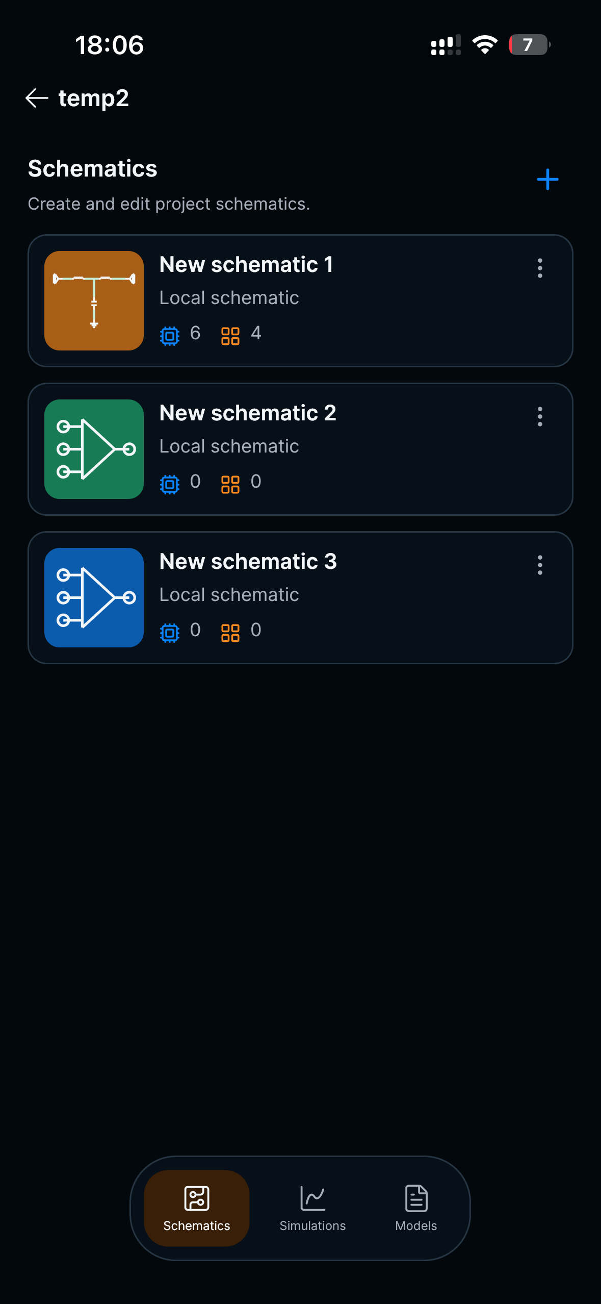
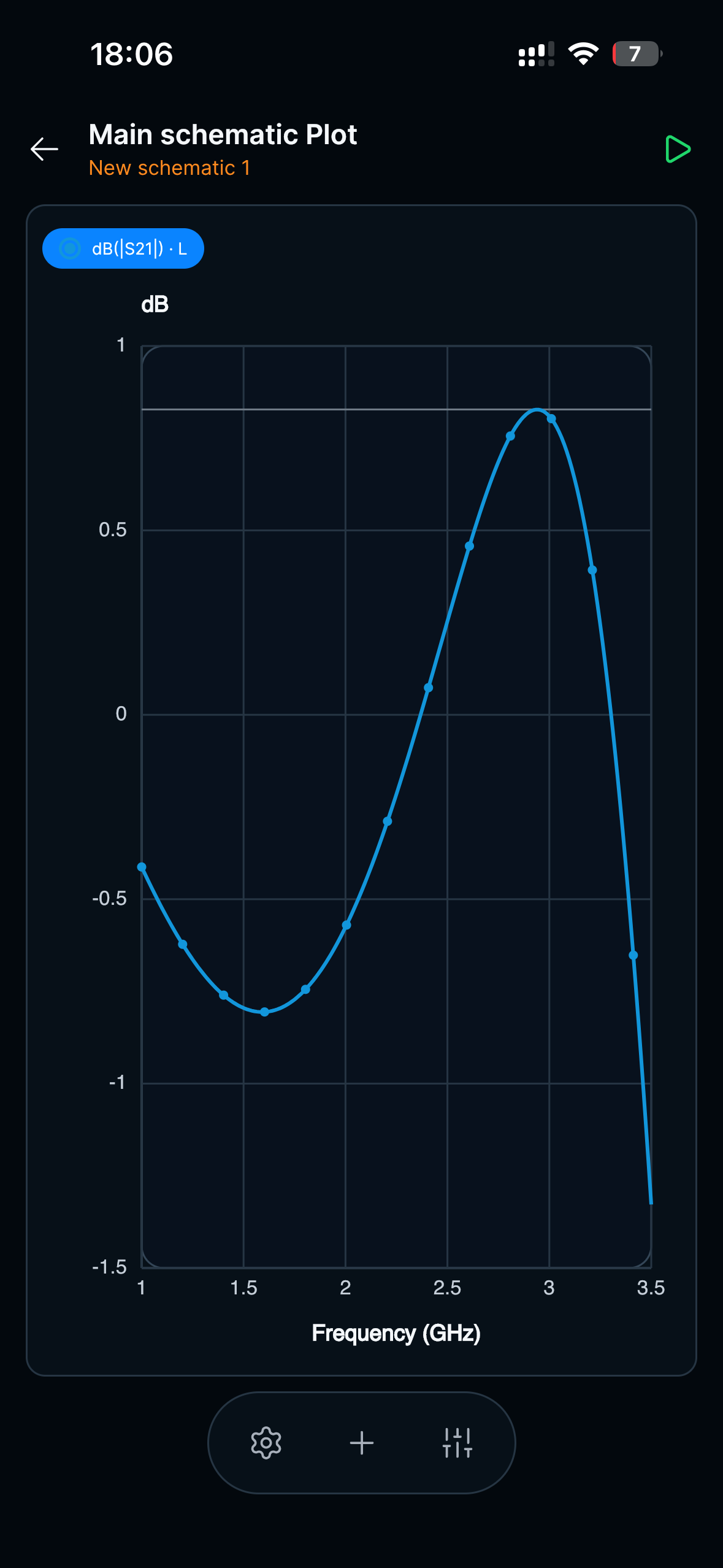
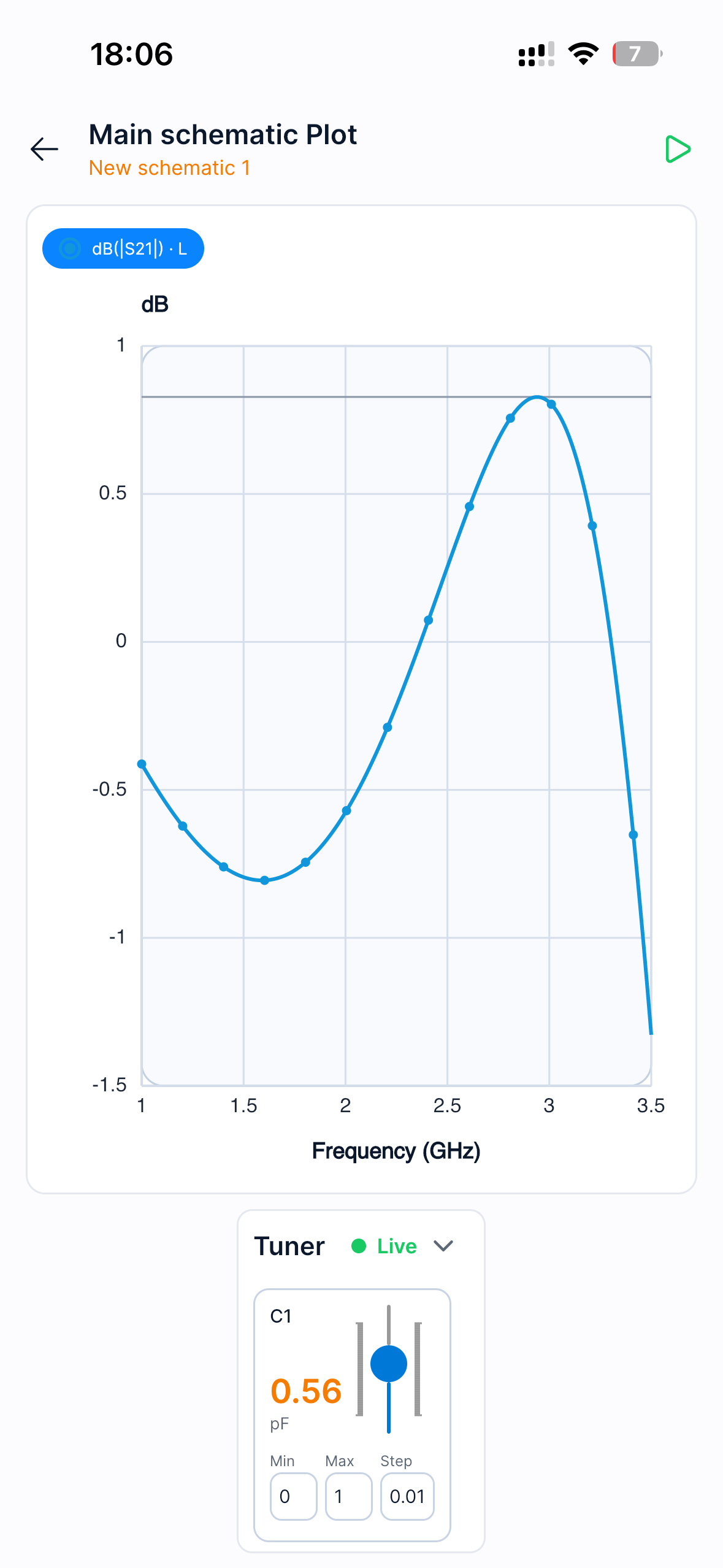
프로젝트, 회로도 편집, RF 플롯, Smith 차트, 튜닝의 실제 앱 화면.
Beta testing
엔지니어, 학생, RF/아날로그 팀이 초기 빌드를 시험하고 무엇을 먼저 다듬어야 할지 알려주길 기다리고 있습니다.
아직 아닙니다. Tersa EDA은 회로도 캡처, 회로 시뮬레이션, 측정, 플롯, 아날로그/RF 튜닝에 집중합니다.
아니요. 빠른 회로 실험, 모바일 검토, RF/아날로그 튜닝을 위한 가벼운 워크스페이스입니다.
첫 버전은 아날로그 회로, AC 및 과도 분석, S-파라미터, Smith 차트, 부품 튜닝에 집중합니다.
아니요. 인터페이스는 모바일, 태블릿, 데스크톱 화면을 위해 설계되었습니다.
Tersa EDA은 회로 분석을 위해 SPICE-compatible workflow를 사용합니다.