

Editor de esquemas
Editor de esquemas
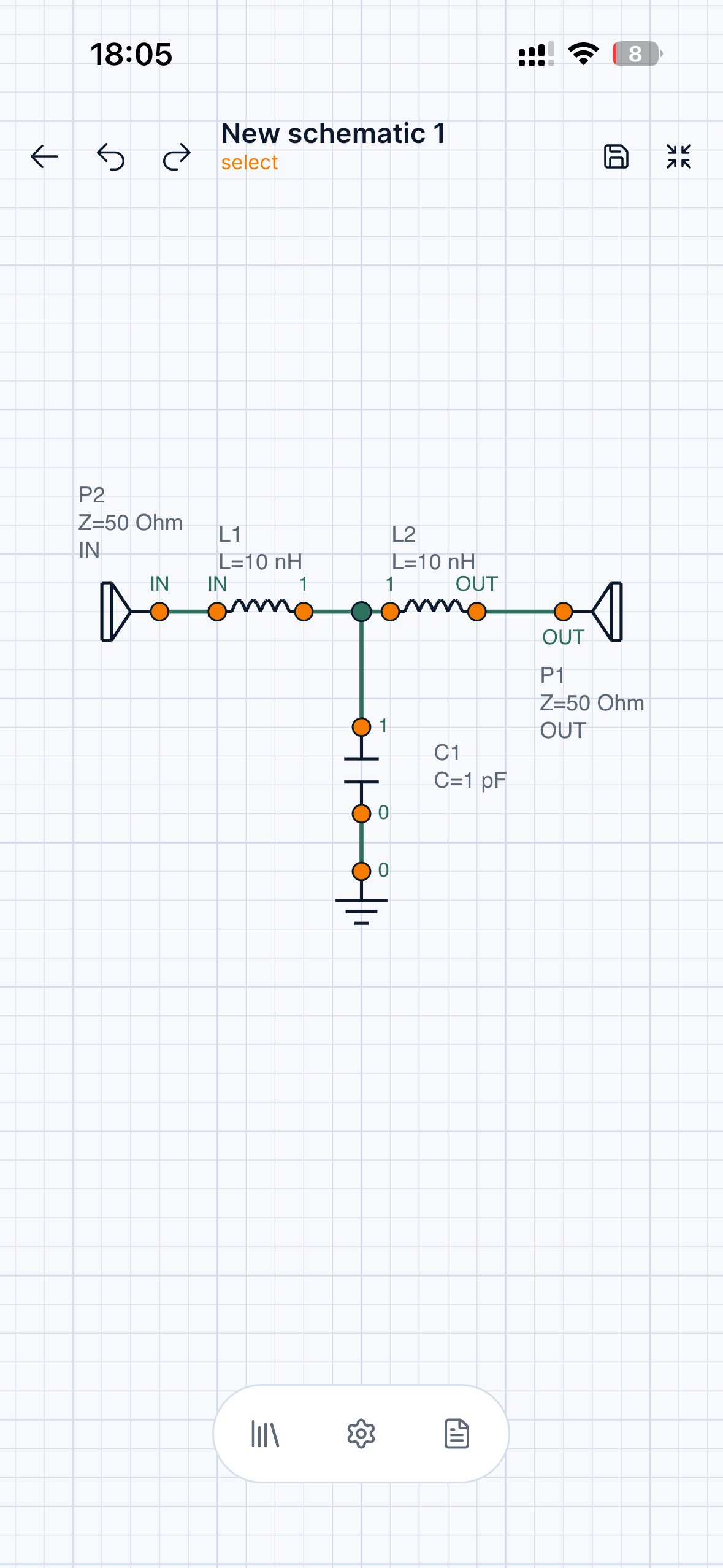
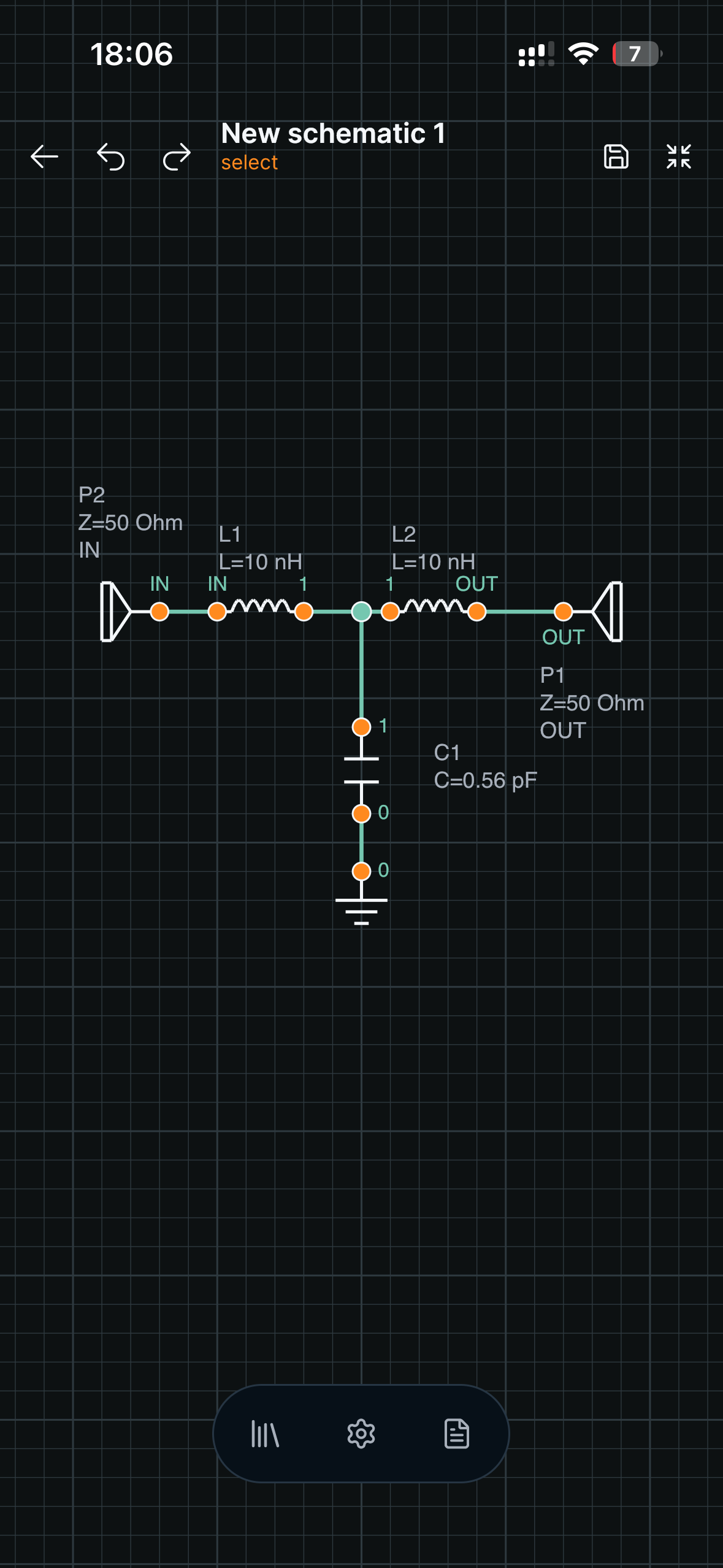
Dibuja circuitos analógicos y RF con puertos, componentes, etiquetas de red y edición táctil.
Tersa EDA · RF / analog
Tersa EDA es una app móvil y de escritorio para crear esquemas, ejecutar simulaciones de circuitos, ajustar componentes e inspeccionar mediciones RF.
Prueba del producto
Construye un esquema, elige un análisis, añade mediciones y ajusta valores sin salir de tu dispositivo.
Editor de esquemas
Dibuja circuitos analógicos y RF con puertos, componentes, etiquetas de red y edición táctil.
Mediciones
Inspecciona trazas, marcadores, respuesta en frecuencia y mediciones derivadas.
RF
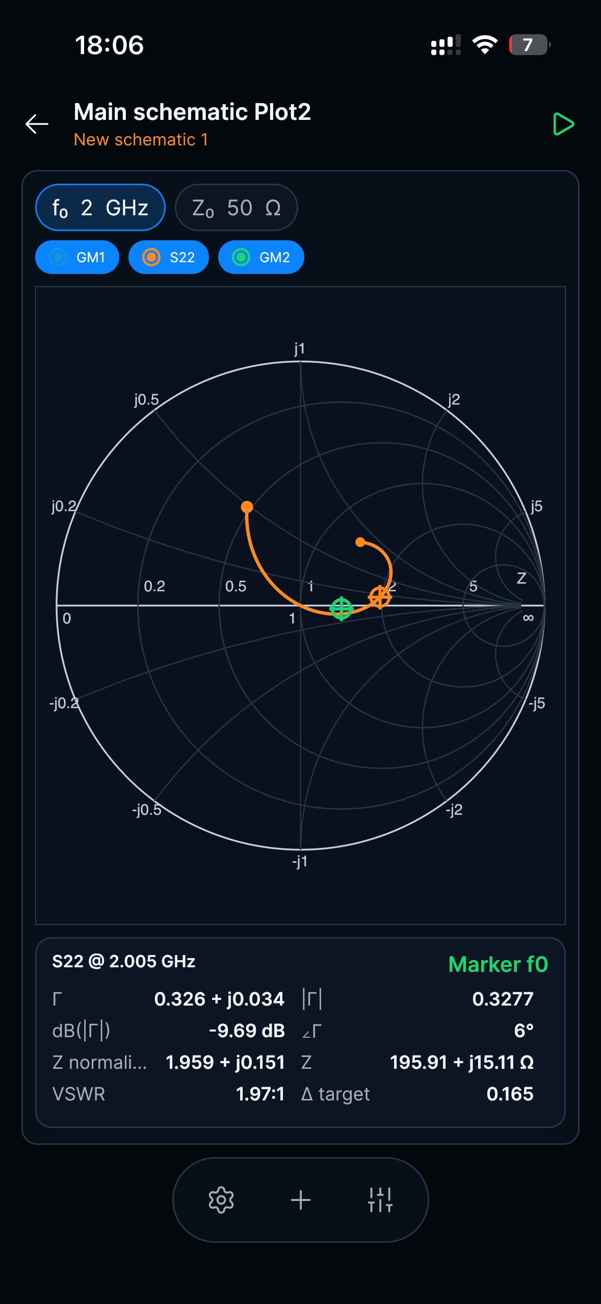
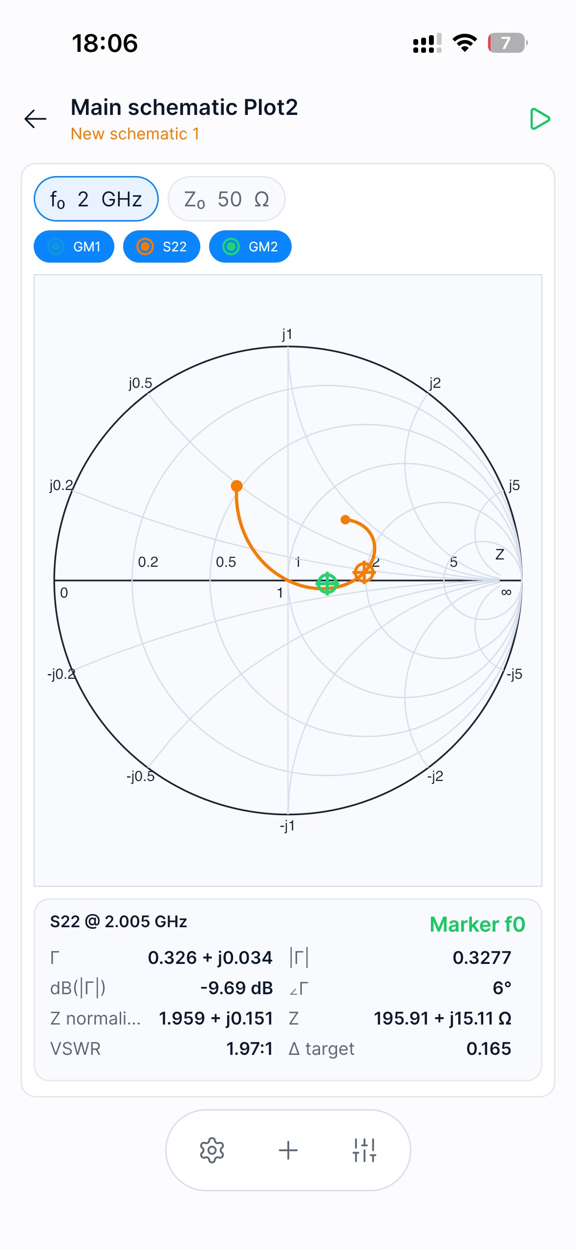
Analiza parámetros S, return loss, insertion loss, impedancia y trayectorias en carta de Smith.
Updated July 27, 2026
Tersa EDA is an RF and analog circuit simulation workspace for engineers, students, and hardware teams who need a focused schematic-to-measurement flow. It combines schematic capture, SPICE-compatible analysis setup, plots, RF measurements, Smith chart inspection, and component tuning in one product surface. The goal is not to replace large desktop EDA suites. The product is designed for quick experiments, tablet review, mobile debugging, and focused circuit tuning when the important question is how the response changes after a component value, port, or measurement is adjusted.
Tersa EDA presents RF results around practical measurements: S11, S21, S12, S22, return loss, insertion loss, gain, stability-oriented traces, frequency markers, and Smith chart trajectories. The workflow starts from the schematic, adds ports and analysis settings, then keeps the plot and tuner connected to the circuit. This makes it useful for filters, matching networks, resonators, small-signal experiments, and quick RF review where the designer needs to compare traces instead of exporting data between separate tools.
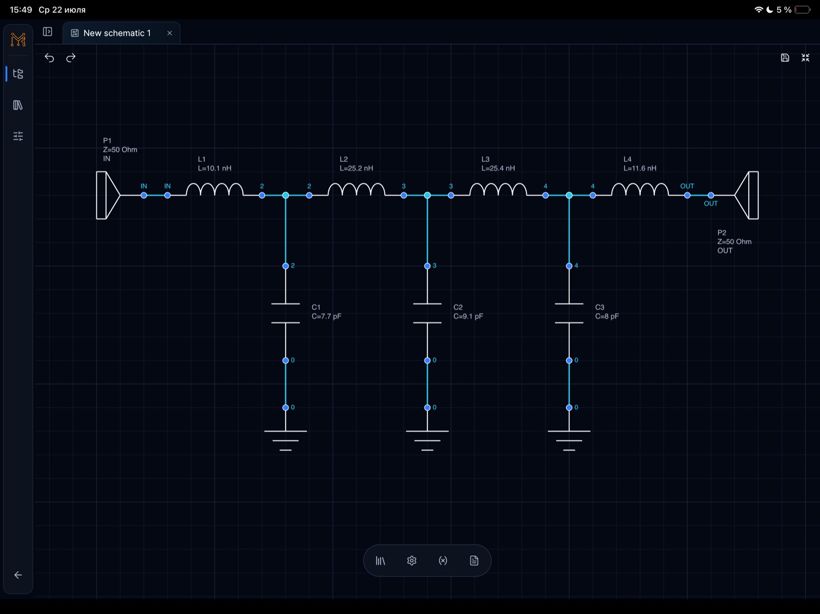
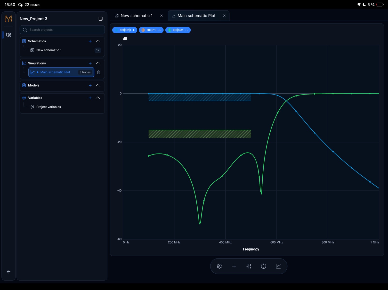
The 500 MHz low-pass filter example demonstrates a complete RF workflow on iPad. It shows a 50 ohm ladder filter with series inductors, shunt capacitors, input and output ports, S-parameter simulation to 1 GHz, insertion loss, return loss, and component tuning. The blue S21 trace shows passband behavior and roll-off, while the green S11 and S22 traces help inspect matching. The tuning sweep makes cutoff movement visible as capacitor and inductor values change around the target frequency.
Funciones
Crea circuitos con componentes, puertos, etiquetas y hojas reutilizables en móvil, tablet o escritorio.
Ejecuta análisis AC, transitorio y RF con gráficas claras, marcadores y controles de trazas.
Inspecciona parámetros S, return loss, insertion loss, cartas de Smith, ganancia y métricas de estabilidad.
Ajusta valores de componentes y ve de inmediato cómo cambia la respuesta del circuito.
La simulación SPICE, las mediciones tipadas, la optimización acotada, Touchstone 1.x y la generación de circuitos editables están activas en producción. El balance armónico, EM y la síntesis RF más amplia siguen en el roadmap.
https://mcp-api.tersaeda.com/mcp · OAuth 2.1 + PKCE
Disponible ahora
Beta activaAnálisis .op, .dc, .ac, .tran y .noise validados con ngspice aislado, vectores limitados y diagnósticos estables.
Roadmap de la plataforma
Balance armónico
Investigación
Análisis EM
Planificado
Los elementos del roadmap indican dirección de producto y aún no son tools MCP disponibles. El alcance y el orden pueden cambiar.
Flujo de trabajo
Construye un esquema, elige un análisis, añade mediciones y ajusta valores sin salir de tu dispositivo.
Coloca componentes, conecta redes y define puertos.
Ejecuta simulaciones AC, transitorias o RF.
Grafica voltajes, parámetros S, pérdidas y marcadores.
Modifica componentes y compara la respuesta.
Product demos
Videos cortos muestran creación de esquemas, simulación, medición y ajuste en vivo de componentes en Tersa EDA.
Tune an RLC circuit directly on iPhone and watch the response update while component values change.
Abrir en YouTubeCreate an RLC schematic on iPhone, run simulation, and inspect the first measurement workflow.
Abrir en YouTubeUse the iPad workspace to tune resonance and compare circuit response changes on a larger engineering canvas.
Abrir en YouTubeBuild an RLC resonator from scratch on iPad and move from schematic capture into analysis setup.
Abrir en YouTubeRF example
A concrete LPF case study built in Tersa EDA: schematic capture, 50 ohm ports, S-parameter simulation, insertion loss, return loss, and component tuning around a 500 MHz target.
Target
500 MHz LPF
Ports
50 ohm IN / OUT
Analysis
S-parameters to 1 GHz
Workflow
Schematic, plot, tuner
This example shows a lumped 500 MHz low-pass filter workflow, not a generic screenshot gallery. The circuit uses a ladder topology with 50 ohm input and output ports, series inductors, shunt capacitors, and RF measurements plotted from DC to 1 GHz.
The blue S21 trace shows the passband and roll-off, while the green S11/S22 traces help inspect matching and return loss. Tuning sweeps make cutoff movement visible as component values change.
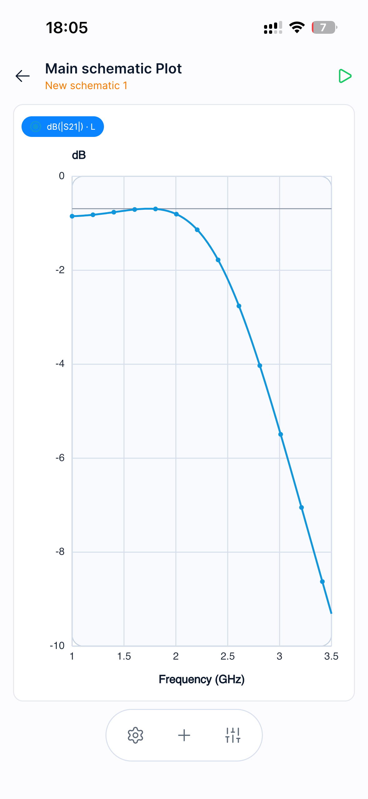
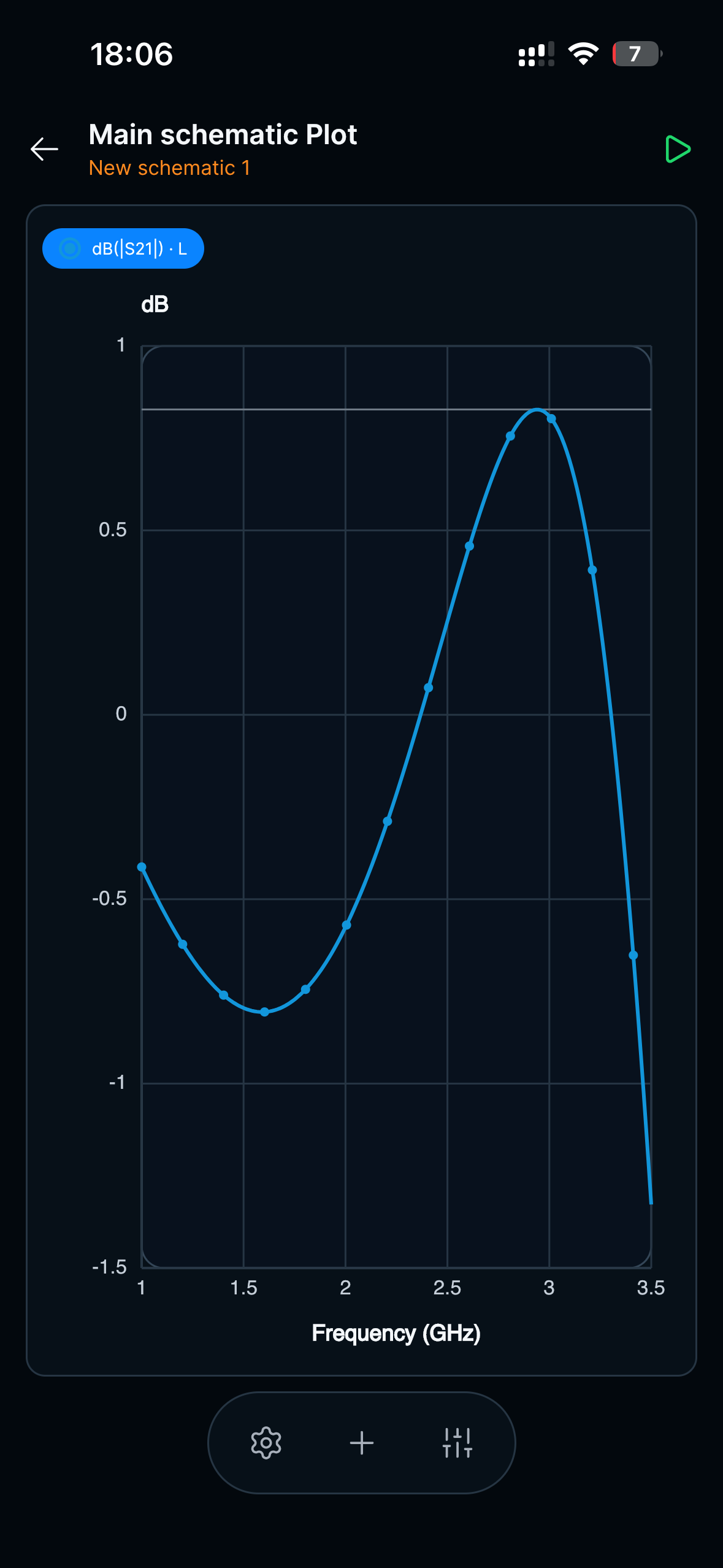
S-parameter response with S21 staying flat through the passband before the transition region toward 1 GHz.
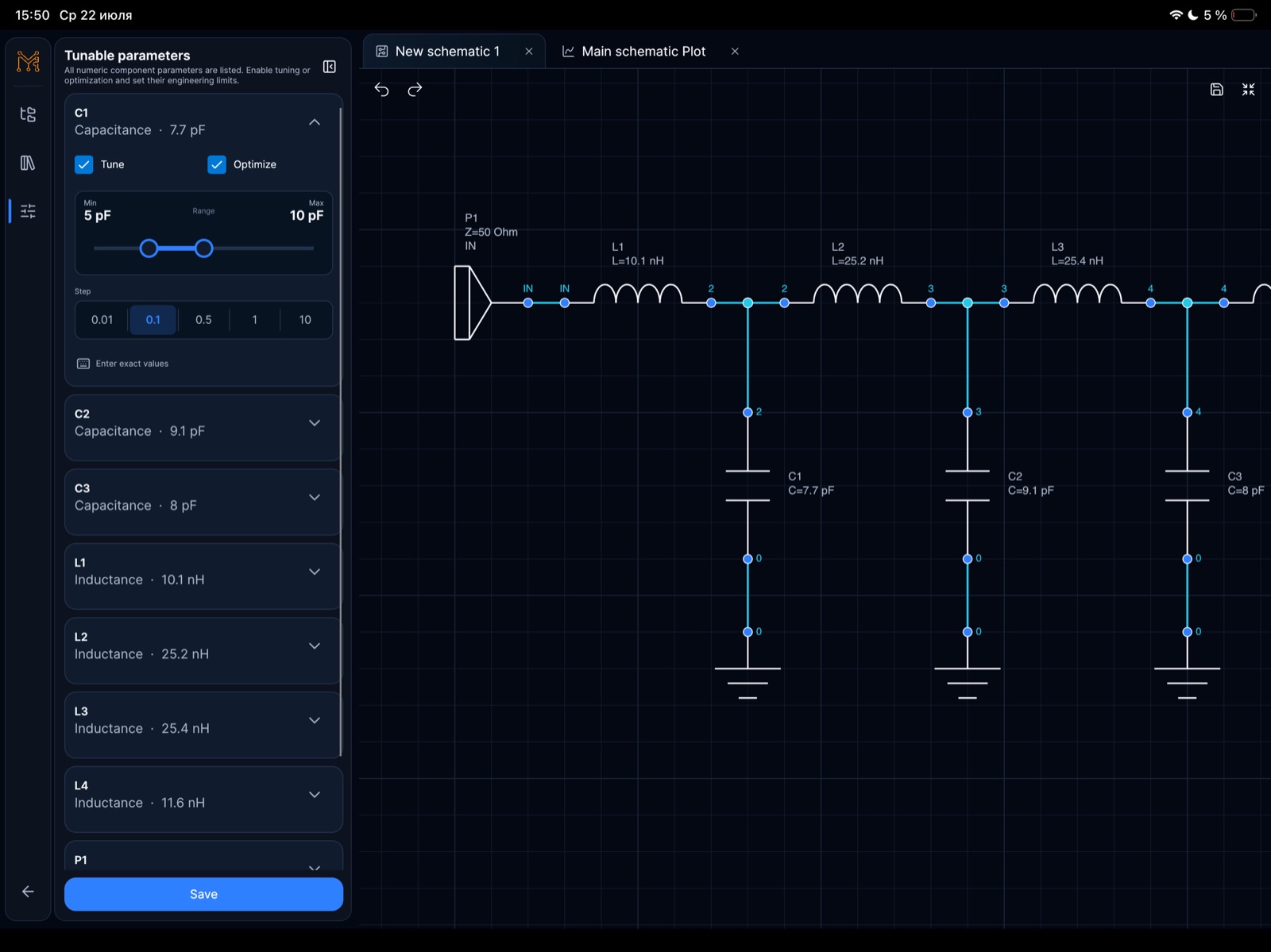
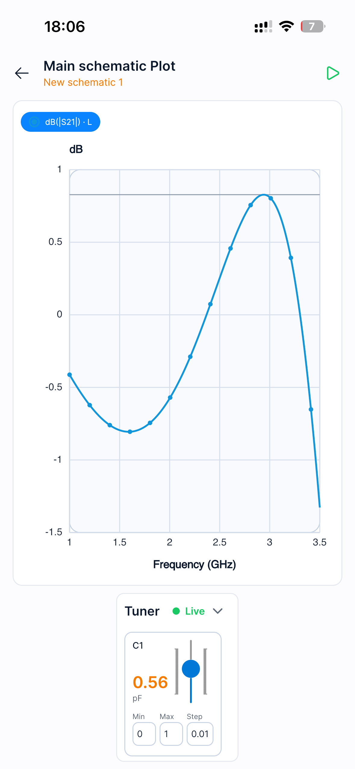
Tuning ranges expose capacitor and inductor values so the cutoff behavior can be optimized directly from the schematic.
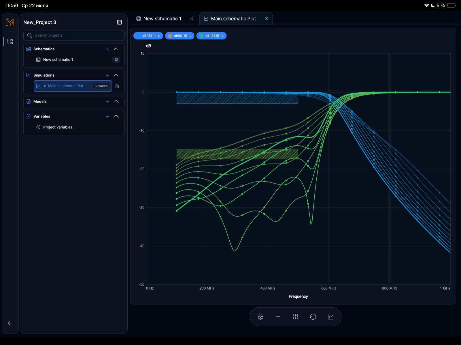
A tuning sweep compares multiple S-parameter traces around the cutoff and stopband regions.
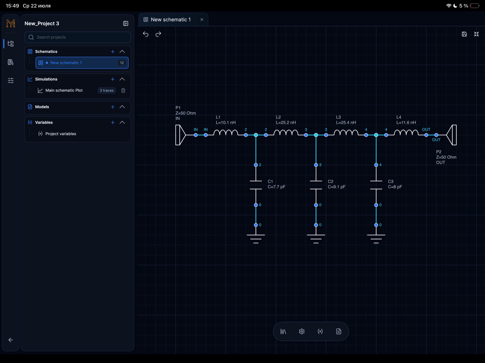
The project workspace keeps the LPF schematic, simulation plot, variables, and tunable parameters in one engineering flow.
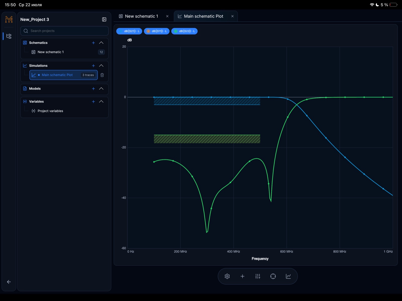
Return loss and insertion loss traces make it possible to inspect passband fit and out-of-band rejection.
Herramientas RF
Tersa EDA incluye mediciones RF junto al trabajo analógico diario: parámetros S, return loss, insertion loss, trayectorias de carta de Smith, métricas de ganancia, estabilidad y marcadores de frecuencia objetivo.
Analógico
Usa Tersa EDA para filtros, divisores, amplificadores, circuitos con diodos, transitorios RC, respuesta en frecuencia y experimentos rápidos de tipo what-if.
Capturas
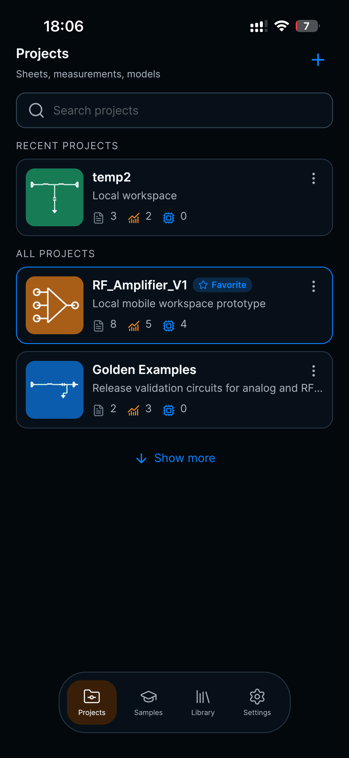
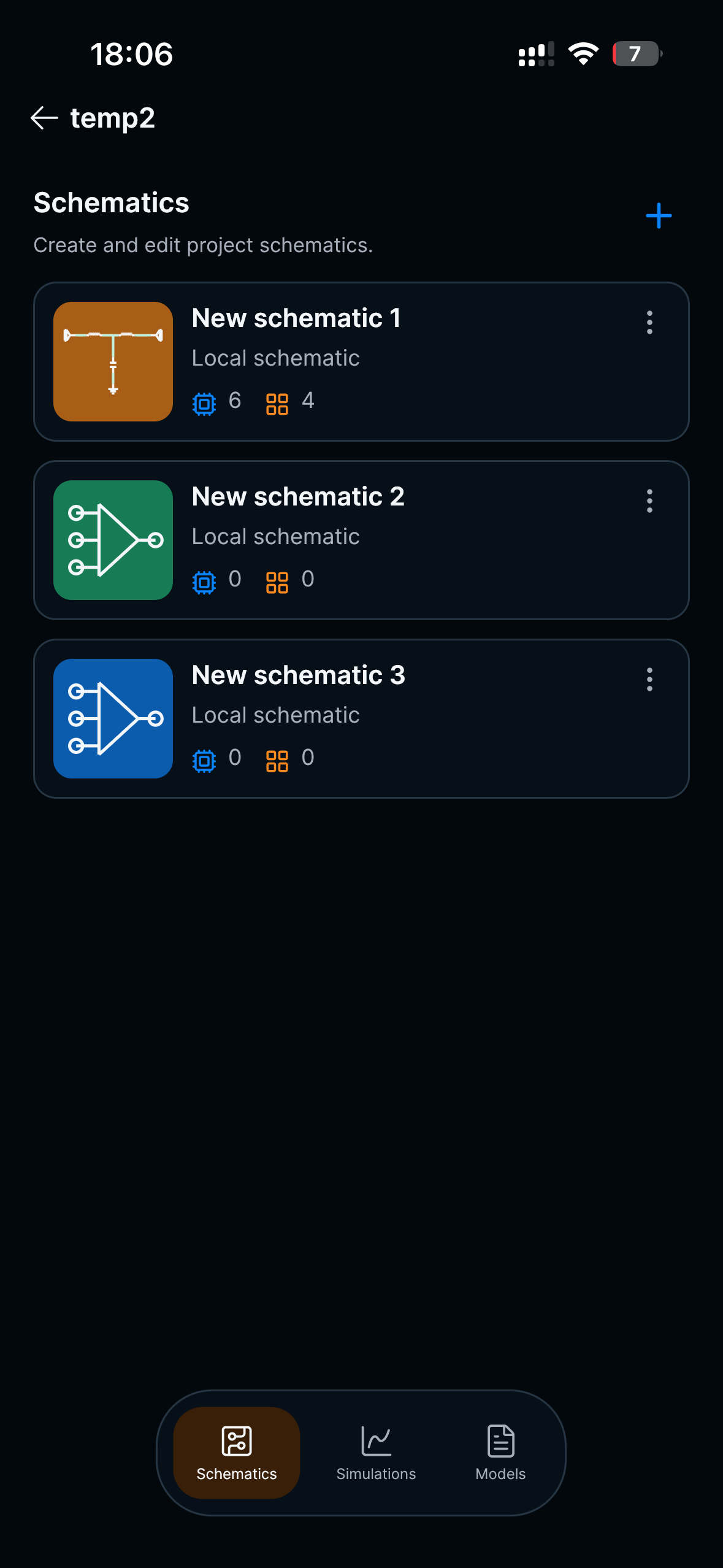
Pantallas reales de proyectos, edición de esquemas, gráficas RF, carta de Smith y ajuste.
Beta testing
Invitamos a ingenieros, estudiantes y equipos RF/analógicos a probar builds tempranas y decirnos qué debemos mejorar primero.
Todavía no. Tersa EDA se centra en captura de esquemas, simulación, mediciones, gráficas y ajuste analógico/RF.
No. Es un workspace ligero para experimentos rápidos, revisión móvil y ajuste RF/analógico. Complementa herramientas de escritorio.
Las primeras versiones se centran en circuitos analógicos, análisis AC y transitorio, parámetros S, cartas de Smith y ajuste de componentes.
No. La interfaz está diseñada para móvil, tablet y escritorio.
Tersa EDA usa un workflow SPICE-compatible para análisis de circuitos.