Tersa EDA

Tersa EDA RF example

Tune an RF matching network in Tersa EDA

Follow a practical Tersa EDA workflow: prepare RF ports, run an S-parameter sweep, inspect S11 on a Smith chart, tune L and C, and verify bandwidth.

Reviewed: 2026-07-31

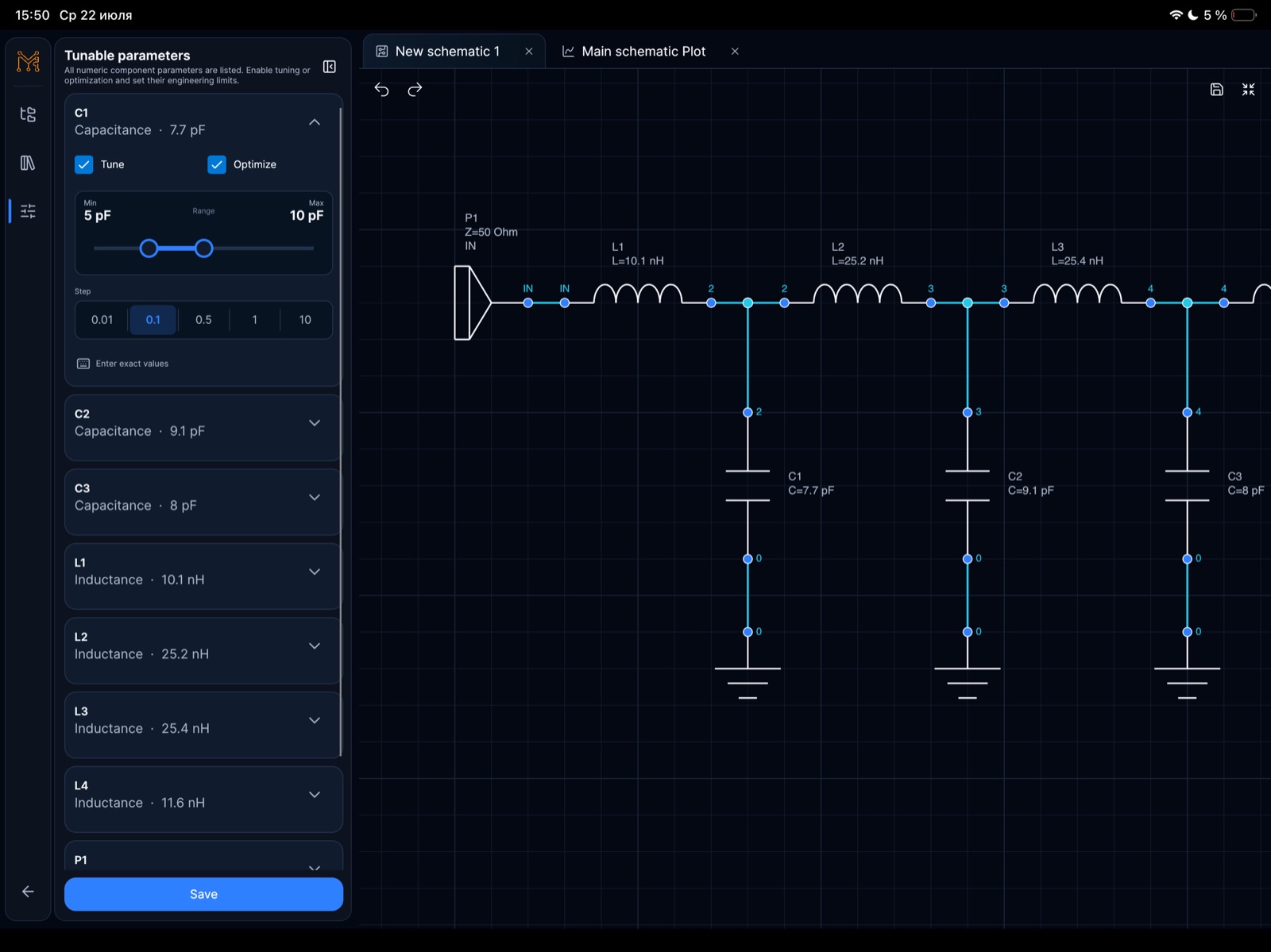
Tunable parameters and RF network schematic in Tersa EDA on iPad

Application workflow

Run the matching loop in Tersa EDA

Use the real product flow to move from a circuit and reference impedance to measured reflection, component tuning, and a verified frequency sweep.

Step 1

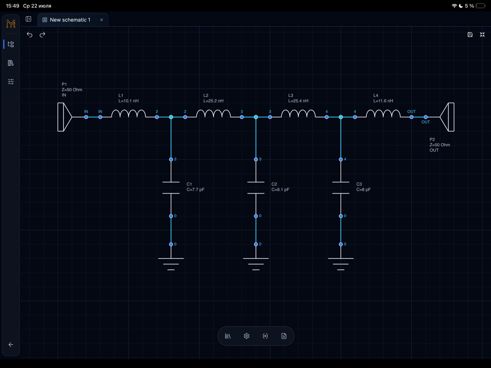
Open the RF example or prepare two ports

For the shortest path, open Golden Examples → Schematics → LC Low-Pass S-Parameters. In a new schematic, use one IN and one OUT port on different nets, normally with a 50 Ω reference impedance. Place the matching components at the intended reference plane.

  • Start from the verified two-port example
  • Confirm port orientation and ground
  • Check every initial L and C value
RF schematic with 50 ohm IN and OUT ports and reactive network in Tersa EDA

Step 2

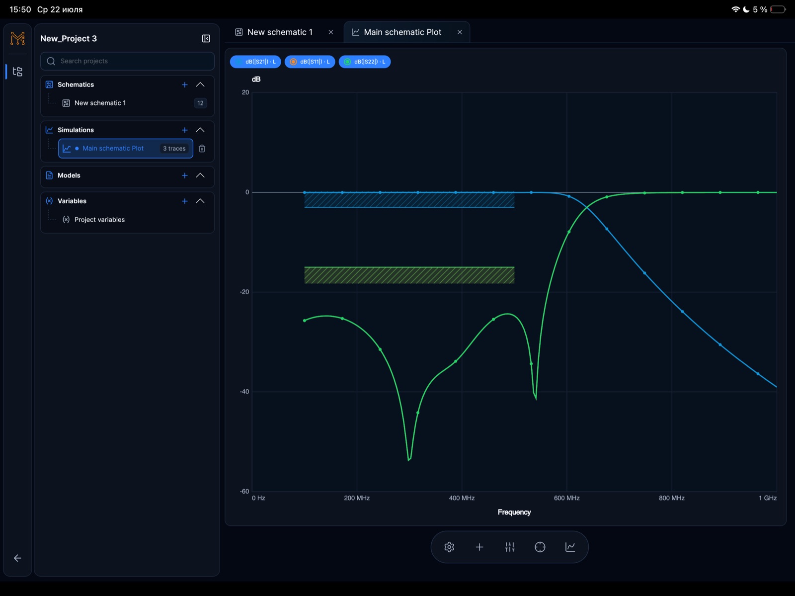
Configure AC and add S11

Create a Rectangular plot, open Properties → Analysis Setup, select AC, and set Start Frequency, Stop Frequency, Points, Sweep Type, Marker f0, and Reference impedance. Then use Add → Port parameters → S11. Add S21 or the return-loss and insertion-loss measurements when the specification needs them.

  • Keep the same sweep for every comparison
  • Record the unmatched S11 baseline
  • Touch the graph to inspect the nearest frequency point
S-parameter frequency response with S11 and S21 traces in Tersa EDA

Step 3

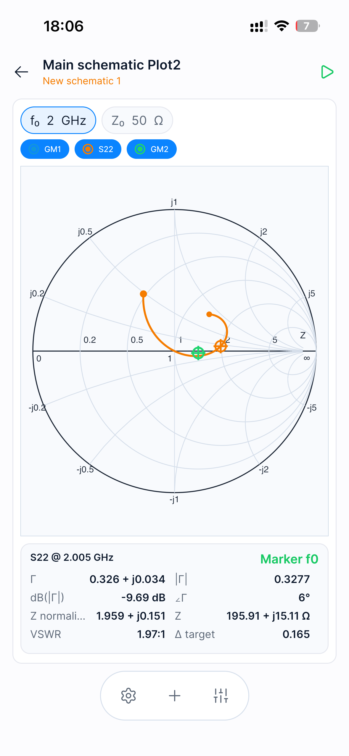
Inspect S11 on the Smith chart

Create a Smith Chart plot and use Add → Reflection / Γ → S11. In Properties, set Marker frequency and enable Show marker details. The readout reports Γ, |Γ|, dB(|Γ|), phase, normalized impedance, physical impedance, and VSWR at the nearest sweep point.

  • Use S11 for the input match
  • Set the marker to the design frequency
  • Read the load character before changing components
Tersa EDA Smith chart with frequency marker, impedance, reflection coefficient, and VSWR readouts
The marker values shown are current; some controls in this earlier beta screenshot have since moved into Properties.

Step 4

Define practical tunable values

Return to the schematic and open Tunable parameters. Enable Tune only for the L or C values that should move, then set realistic Min, Max, and Step values or enter exact values. Save the setup before returning to the plot.

  • Start with one or two variables
  • Use purchasable ranges and increments
  • Keep unrelated components fixed
Tunable parameters panel with Tune, minimum, maximum, and step controls in Tersa EDA

Step 5

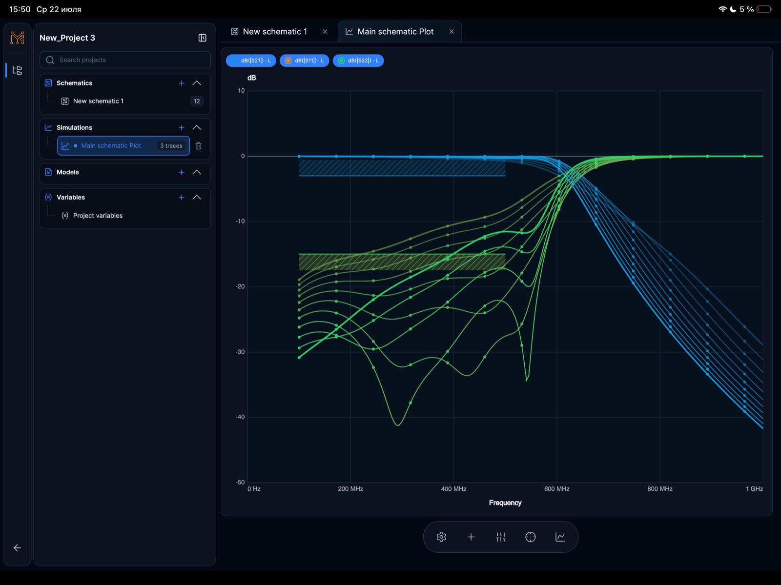
Tune, sweep, and verify the band

Open Tuner in the Rectangular or Smith plot and change L or C with the value field, slider, or −/+ controls. Tersa automatically recalculates after each change. For a family of curves, open Parameter sweep, choose one parameter and Start, Stop, and Step, then run the sweep in a Rectangular plot.

  • Watch the complete S11 trajectory, not one point
  • Check the target and both band edges
  • Confirm S21 remains acceptable
  • Record the selected values and physical verification plan
Tersa EDA rectangular parameter sweep showing RF response across component values

Target

defined Z0 and band

Measurements

S11 + Smith chart

Controls

tunable L and C

Decision

match + bandwidth

Start with an explicit specification

Before moving a slider, define the reference impedance, target frequency, operating band, maximum acceptable S11 or VSWR, and any insertion-loss limit. Tuning without these limits can produce an attractive center point that does not solve the real design requirement.

  • Write the target before opening the tuner
  • Keep the same sweep and reference impedance
  • Tune the smallest practical set of variables
  • Save the baseline marker values

Treat simulation as the design loop, not final proof

Tersa can make the schematic-to-measurement loop fast, but the final network still depends on component Q, package and layout parasitics, connector transitions, and the measured device impedance. Use simulation to find a robust candidate and plan the physical tuning range.

  • Prefer available component values
  • Leave room for board-level adjustment
  • Export or record before-and-after values
  • Verify the built network with calibrated RF measurements

Primary sources

Verify the RF principles

Definitions and matching guidance are grounded in the engineering documentation below. Always validate a simulated match with realistic models and measurements.

FAQ

Can I tune every component at once?

You can expose multiple tunable parameters, but a small deliberate set is easier to interpret and less likely to produce impractical combinations.

Should the Smith marker land exactly at the center?

Only if that also satisfies bandwidth, loss, tolerance, and stability requirements. A robust near-center trajectory can be better than a fragile single-point minimum.

What should I record before tuning?

Record the circuit revision, reference impedance, sweep, marker frequencies, baseline S11 or VSWR, and starting component values.

Does this replace VNA verification?

No. The physical network must be verified with calibrated measurements and realistic reference-plane handling.